Semiconductor device with increased I/O leadframe including passive device

a technology of semiconductor devices and leadframes, applied in semiconductor devices, semiconductor/solid-state device details, electrical apparatus, etc., can solve the problems of no existing integration methods, and achieve the effect of effectively electrically isolating various leads from each other within the semiconductor package, and maximizing the available number of exposed leads

Active Publication Date: 2011-12-06
AMKOR TECH SINGAPORE HLDG PTE LTD
View PDF439 Cites 12 Cited by
  • Summary
  • Abstract
  • Description
  • Claims
  • Application Information

AI Technical Summary

Benefits of technology

[0010]In accordance with the present invention, there are provided multiple embodiments of a semiconductor package, each embodiment including a uniquely configured leadframe sized and configured to maximize the available number of exposed leads in the semiconductor package. More particularly, each embodiment of the semiconductor package of the present invention includes a generally planar die paddle or die pad defining multiple peripheral edge segments. In addition, the semiconductor package includes a plurality of leads. Some of these leads include exposed bottom surface portions or lands which are provided in at least one row or ring which at least partially circumvents the die pad, with other leads including portions which protrude from respective side surfaces of a package body of the semiconductor package. Connected to the top surface of the die pad is at least one semiconductor die which is electrically connected to at least some of the leads. A passive device may be electrically connected to and extend between the die pad and one of the leads, and / or may be electrically connected to and extend between and adjacent pair of the leads. At least portions of the die pad, the leads, the passive device(s), and the semiconductor die are encapsulated by the package body, with at least portions of the bottom surfaces of the die pad and some of the leads being exposed in a common exterior surface of the package body. The leadframe of the semiconductor package is fabricated in accordance with standard, low-cost forming techniques. In accordance with the present invention, sawing, punching, etching, or other material removal processes may be completed during the fabrication of the semiconductor package to effectively electrically isolate various leads from each other within the semiconductor package. The semiconductor package of the present invention may include one or more internal semiconductor dies, depending on functional requirements.

Problems solved by technology

Though it is known in the prior art to integrate passive components into laminate and leadframe based semiconductor packages, none of the existing integration methods result in a semiconductor package configuration wherein at least one pad is provided on the semiconductor package and dedicated to the passive component for connectivity purposes.

Method used


Image

  • Semiconductor device with increased I/O leadframe including passive device
  • Semiconductor device with increased I/O leadframe including passive device
  • Semiconductor device with increased I/O leadframe including passive device

Examples


first embodiment

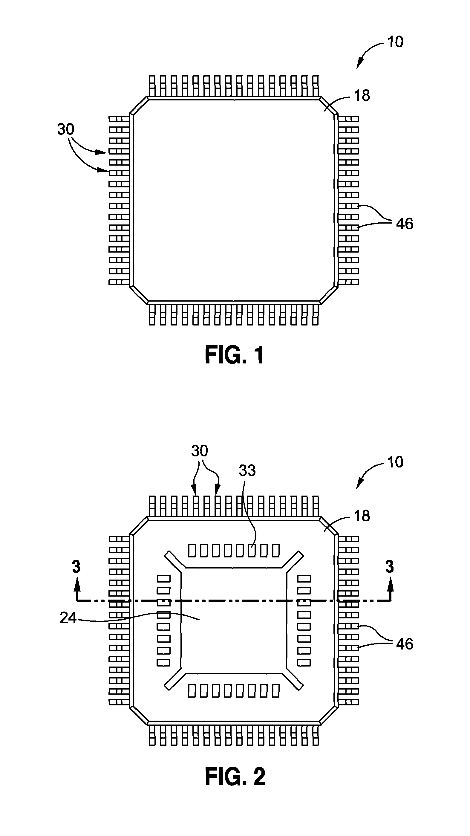
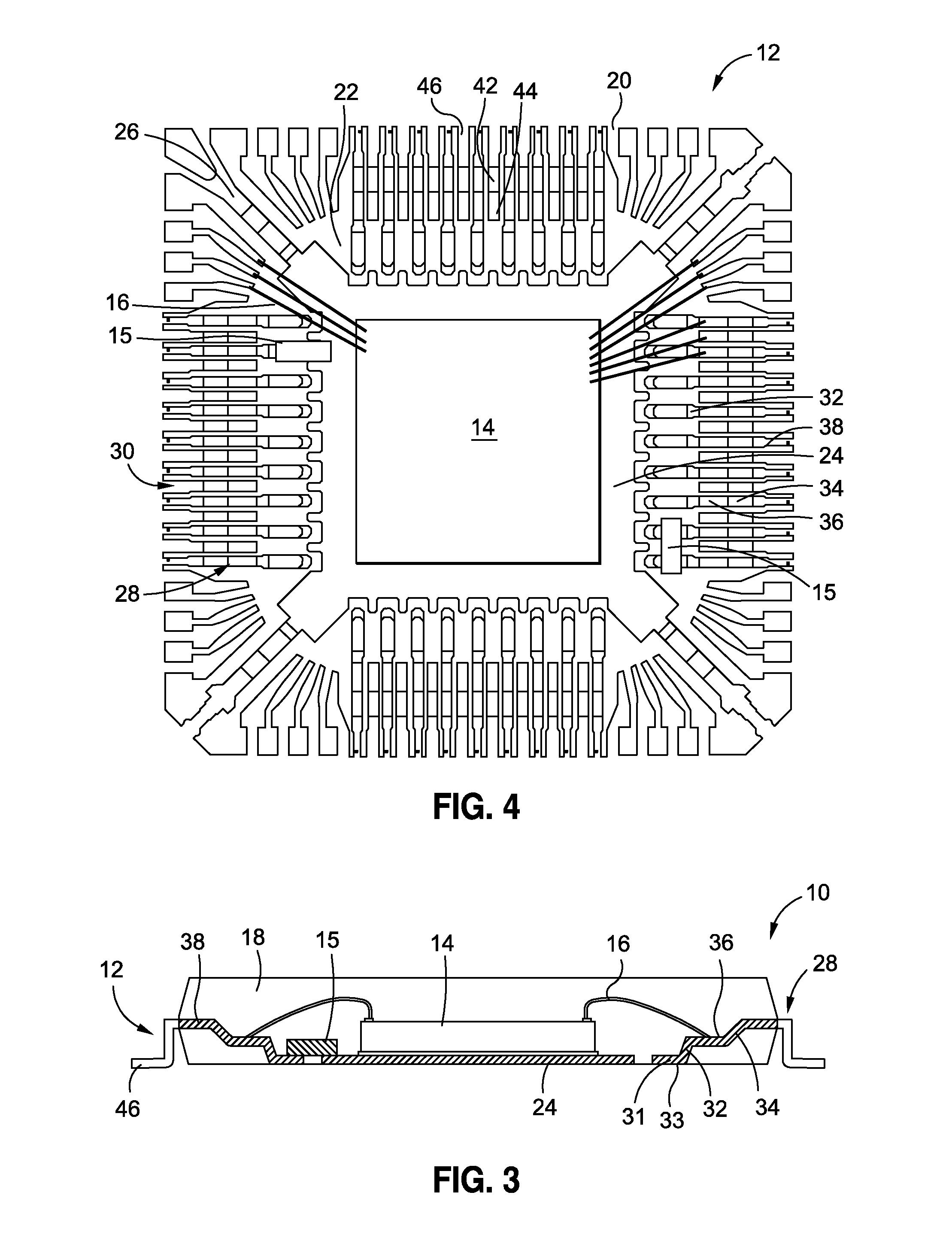
[0028]Referring now to the drawings wherein the showings are for purposes of illustrating various embodiments of the present invention only, and not for purposes of limiting the same, FIGS. 1-5 depict a semiconductor package 10 constructed in accordance with the present invention. The major structural elements of the semiconductor package 10 include a leadframe 12 (shown in FIG. 4), a semiconductor die 14 attached to the leadframe 12 and electrically connected thereto by conductive wires 16, at least one passive component 15 electrically connected to the leadframe 12, and a package body 18 which fully encapsulates the semiconductor die 14, the passive component 15 and wires 16, and partially encapsulates the leadframe 12 in a manner which will be described in more detail below.

[0029]The leadframe 12 of the semiconductor package 10 includes a peripheral outer dambar 20 which defines a central opening 22. Located within the central opening 22 is a generally quadrangular die pad 24 of ...

second embodiment

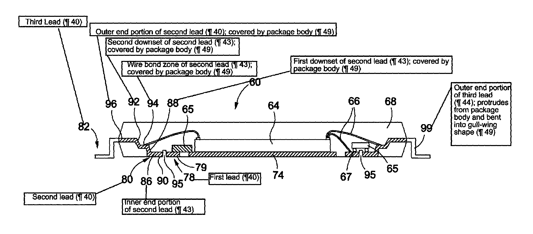
[0040]Referring now to FIGS. 6-9, there is depicted a semiconductor package 60 constructed in accordance with the present invention. The major structural elements of the semiconductor package 60 include a leadframe 62, a semiconductor die 64 attached to the leadframe 62 and electrically connected thereto by conductive wires 66, at least one passive component 65 electrically connected to the leadframe 62, and a package body 68 which fully encapsulates the semiconductor die 64, the passive component 65, and wires 66 and partially encapsulates the leadframe 62 in a manner which will be described in more detail below.

[0041]As best seen in FIG. 9, the leadframe 62 of the semiconductor package 60 includes a peripheral outer dambar 70. Located within outer dambar 70 is a continuous, generally quadrangular tie ring 72. Disposed within the tie ring 72 is a generally quadrangular die pad 74 of the leadframe 62. The die pad 74 defines opposed, generally planar top and bottom pad surfaces, and ...

third embodiment

[0054]Referring now to FIGS. 10, 11 and 12, there is depicted a semiconductor package 100 constructed in accordance with the present invention. The major structural elements of the semiconductor package 100 include a leadframe 102, a semiconductor die 104 attached to the leadframe 102 and electrically connected thereto by conductive wires 106, one or more passive components 107 mounted and electrically connected to the leadframe 102, and a package body 108 which fully encapsulates the semiconductor die 104, the passive components(s) 107 and wires 106, and partially encapsulates the leadframe 102 in a manner which will be described in more detail below. In FIG. 10, the outline of the package body 108 of the semiconductor package 100 is shown in phantom so as to provide an unobstructed view of the leadframe 102, semiconductor package 104 attached thereto through the use of the wires 106, and the passive component(s) 107 attached and electrically connected thereto.

[0055]The leadframe 1...


PUM


Abstract

In accordance with the present invention, there are provided multiple embodiments of a semiconductor package, each embodiment including a uniquely configured leadframe sized and configured to maximize the available number of exposed leads in the semiconductor package. More particularly, each embodiment of the semiconductor package of the present invention includes a generally planar die pad and a plurality of leads. Some of these leads include exposed bottom surface portions or lands which are provided in at least one row or ring which at least partially circumvents the die pad, with other leads including portions which protrude from respective side surfaces of a package body of the semiconductor package. A passive device may be electrically connected to and extend between the die pad and one of the leads, and/or may be electrically connected to and extend between and adjacent pair of the leads.

Description

CROSS-REFERENCE TO RELATED APPLICATIONS[0001]Not ApplicableSTATEMENT RE: FEDERALLY SPONSORED RESEARCH / DEVELOPMENT[0002]Not ApplicableBACKGROUND OF THE INVENTION[0003]1. Field of the Invention[0004]The present invention relates generally to integrated circuit chip package technology and, more particularly, to an increased capacity QFP semiconductor package which includes exposed leads and an exposed die pad on the bottom surface of the package body thereof, and further includes one or more integrated passive components or devices to enhance electrical performance and reduce the number of component parts needed on an underlying printed circuit board or motherboard.[0005]2. Description of the Related Art[0006]Semiconductor dies are conventionally enclosed in plastic packages that provide protection from hostile environments and enable electrical interconnection between the semiconductor die and an underlying substrate such as a printed circuit board (PCB) or system board. The elements ...

Claims


Application Information

Patent Timeline
Patent Type & Authority Patents(United States)
IPC IPC(8): H01L21/4763
CPCH01L23/49541H01L23/49551H01L23/49589H01L2224/48091H01L2224/48247H01L2224/48465H01L2224/49171H01L2924/01013H01L2924/01029H01L2924/01079H01L2924/19041H01L2924/3011H01L2924/00014H01L24/48H01L24/49H01L2924/00H01L2224/49109H01L2224/49433H01L2924/14H01L2924/181H01L2924/30111H01L2924/00012H01L2224/45099H01L2224/45015H01L2924/207
Inventor KARIM, NOZAD O.OLSON, TIMOTHY L.
Owner AMKOR TECH SINGAPORE HLDG PTE LTD
Why Eureka
Try Eureka