Increased I/O leadframe and semiconductor device including same

a semiconductor and leadframe technology, applied in semiconductor devices, semiconductor/solid-state device details, electrical apparatus, etc., can solve the problems of increasing the overall size of the qfp package, further limiting the number of inputs/outputs (i/o's) which may be included therein, and conventional leadframe structures as currently known and integrated into existing qfp packages often prove unsatisfactory, so as to achieve the effect of effectively electrically isolating various leads from each

Active Publication Date: 2011-08-02
AMKOR TECH SINGAPORE HLDG PTE LTD
View PDF442 Cites 22 Cited by
  • Summary
  • Abstract
  • Description
  • Claims
  • Application Information

AI Technical Summary

Benefits of technology

[0013]In accordance with the present invention, there is provided a semiconductor package (e.g., a QFP package) including a uniquely configured leadframe sized and configured to maximize the available number of exposed leads in the semiconductor package. More particularly, the semiconductor package of the present invention includes a generally planar die pad or die paddle defining multiple peripheral edge segments. In addition, the semiconductor package includes a plurality of leads. Some of these leads include exposed bottom surface portions which are provided in at least two concentric rows or rings which at least partially circumvent the die pad, with other leads including portions which protrude from respective side surfaces of a package body of the semiconductor package. Connected to the top surface of the die pad is at least one semiconductor die which is electrically connected to at least some of the leads. At least portions of the die pad, the leads, and the semiconductor die are encapsulated by the package body, with at least portions of the bottom surfaces of the die pad and some of the leads being exposed in a common exterior surface of the package body. The leadframe of the semiconductor package is fabricated in accordance with standard, low-cost forming techniques. In accordance with the present invention, sawing, punching, etching, or other material removal processes may be completed during the fabrication of the semiconductor package to effectively electrically isolate various leads from each other within the semiconductor package. The semiconductor package of the present invention may include one or more internal semiconductor dies, depending on functional requirements.

Problems solved by technology

One of the deficiencies of currently known QFP packages is attributable to the length at which the leads protrude from the sides of the package body, such protrusion length resulting in an increase in the overall size of the QFP package and further limiting the number of inputs / outputs (I / O's) which may be included therein.
In view of this need, conventional leadframe structures as currently known and integrated into existing QFP packages often prove to be unsatisfactory.
However, the circuit boards integrated into these types of semiconductor packages are expensive and typically exhibit poor heat sink and electrical performance characteristics in comparison to semiconductor packages employing leadframes.
Such a structure is difficult to achieve in a semiconductor package employing a circuit board.

Method used


Image

  • Increased I/O leadframe and semiconductor device including same
  • Increased I/O leadframe and semiconductor device including same
  • Increased I/O leadframe and semiconductor device including same

Examples


second embodiment

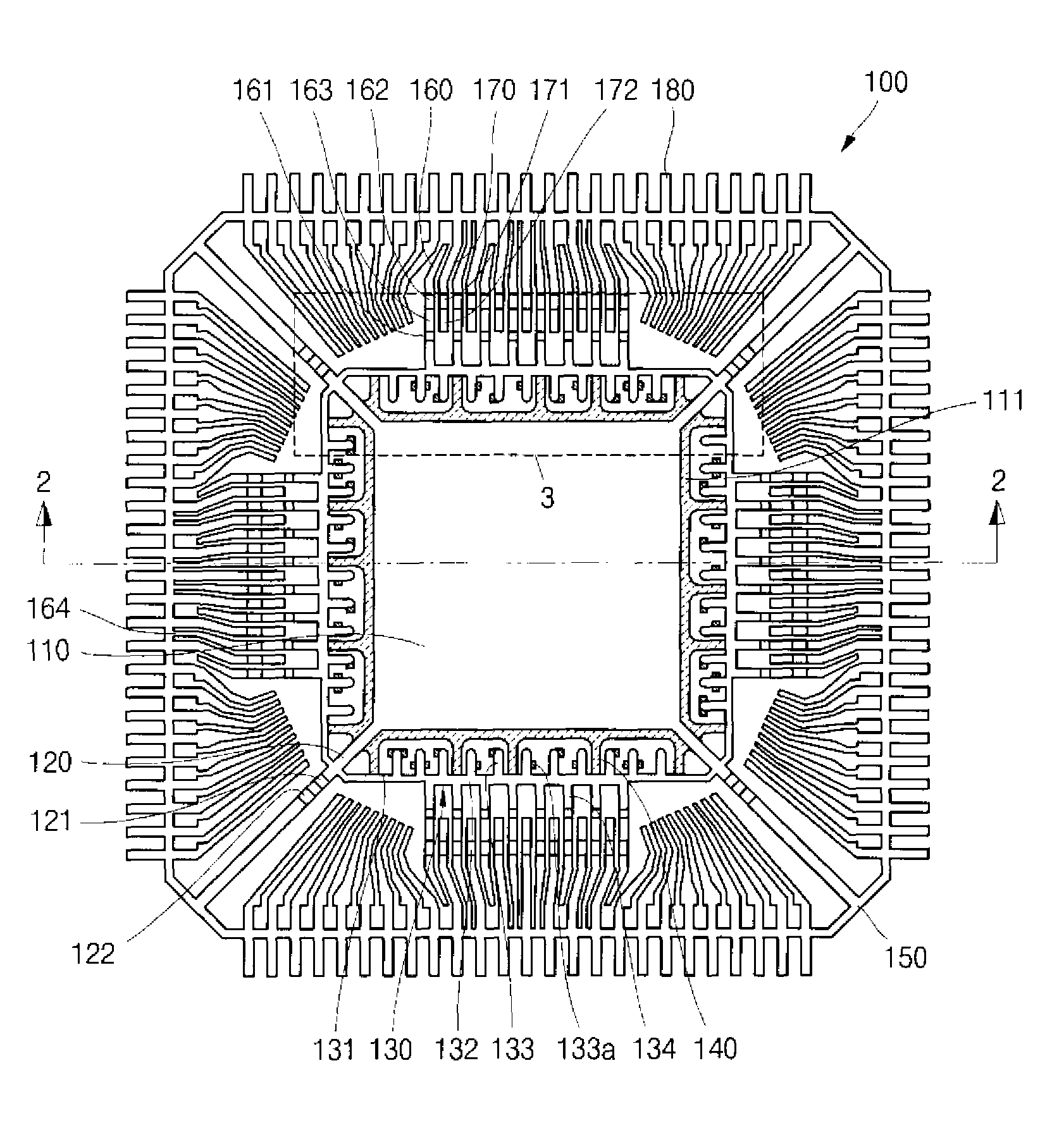
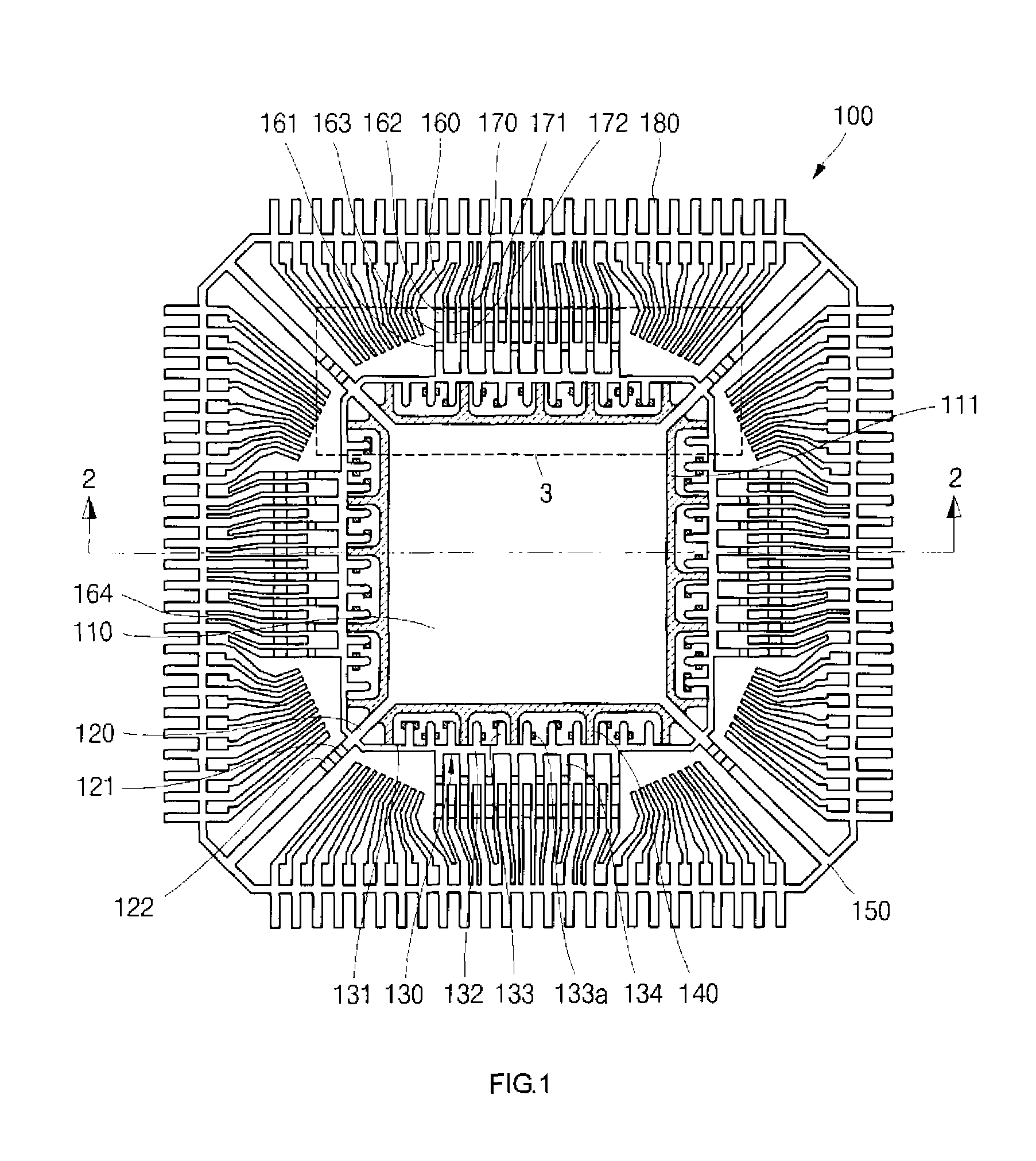
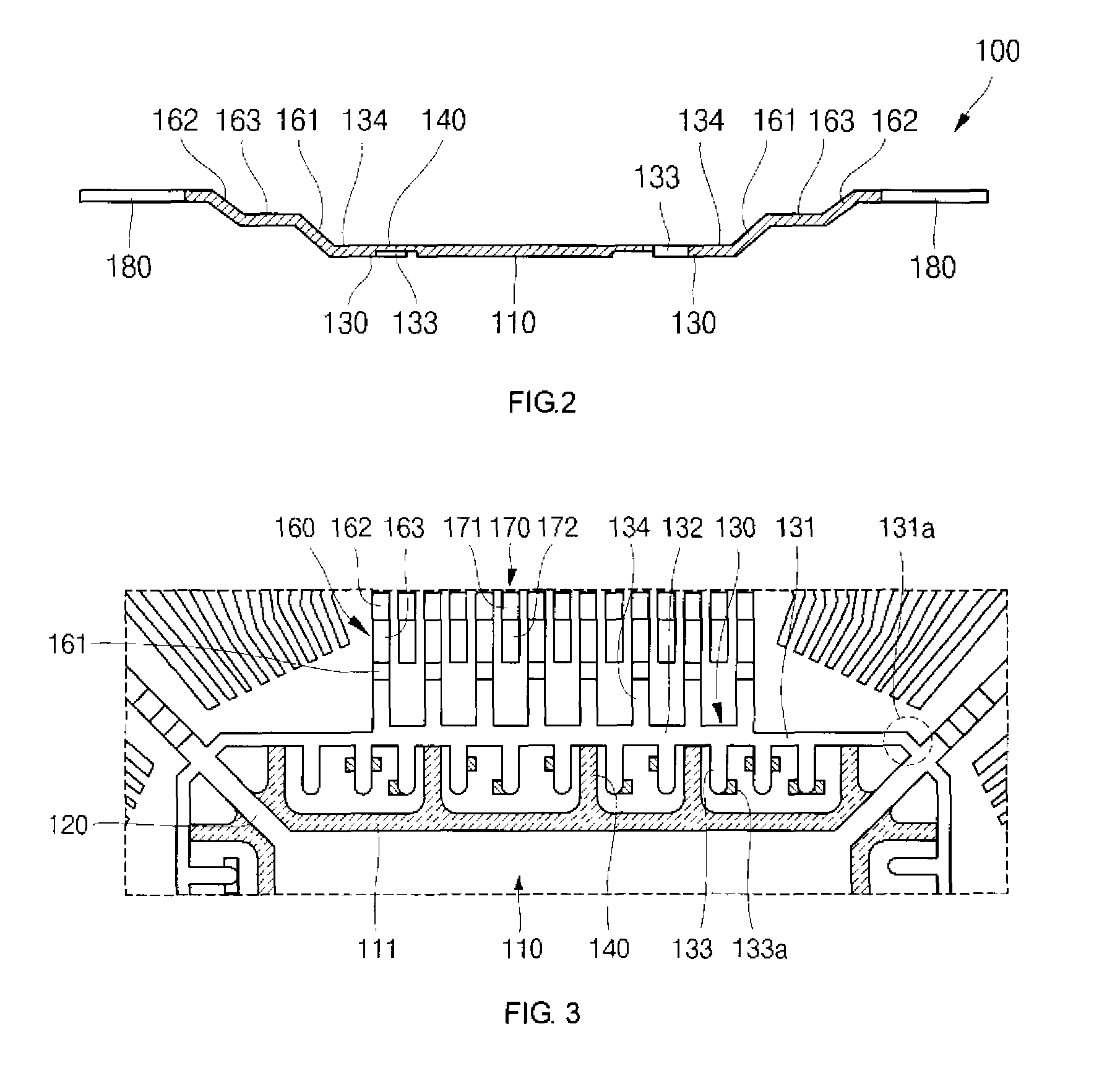
[0073]Referring now to FIG. 4, there is shown a leadframe 200 constructed in accordance with the present invention. The leadframe 200 is substantially similar in structure to the leadframe 100, with only the differences between the leadframes 100, 200 being described below.

[0074]The sole distinction between the leadframes 100, 200 lies in the structural attributes of the land connecting bar 230 of the leadframe 200, in comparison to the land connecting bar 130 of the leadframe 100. As seen in FIG. 4, each of the four peripheral segments of the land connecting bar 230 includes a spaced pair of outer portions 131, and a central portion 232 which extends between and interconnects the outer portions 131. However, in contrast to the linear configuration of the central portion 132 of each peripheral segment of the land connecting bar 130, the central portion 232 of each peripheral segment of the land connecting bar 230 has a serpentine or zigzag configuration.

[0075]In the process of fabri...

third embodiment

[0076]Referring now to FIGS. 5 and 6A, there is shown a leadframe 300 constructed in accordance with the present invention. The leadframe 300 is also substantially similar in structure to the leadframe 100, with only the differences between the leadframes 100, 300 being described below.

[0077]The primary structural distinction between the leadframes 100, 300 lies in the structural attributes of the land connecting bar 330 of the leadframe 300 in comparison to the land connecting bar 130 of the leadframe 100. Each of the four peripheral segments of the land connecting bar 330 includes a spaced pair of outer portions 331 and a central portion 332 which extends between and interconnects the outer portions 331. Within each peripheral segment of the land connecting bar 330, the outer portions 331 are of identical width which is less than that of the central portion 332. Additionally, as seen in FIG. 6A, the central portion 332 of each peripheral segment of the land connecting bar 330 may ...

fourth embodiment

[0082]Referring now to FIGS. 7 and 8, there is shown a leadframe 400 constructed in accordance with the present invention. The leadframe 400 is also substantially similar in structure to the leadframe 100, with only the distinctions between the leadframes 100, 400 being described below.

[0083]The sole distinction between the leadframes 100, 400 lies in the structural attributes of the land connecting bar 430 of the leadframe 400 in comparison to the land connecting bar 130 of the leadframe 100. More particularly, in the land connecting bar 430, each of the four peripheral segments (including the central portion 132 and outer portions 131 of each such peripheral segment) include a plurality of concave recesses or dimples 430a formed on the top and / or bottom surfaces thereof. As is best seen in FIG. 8, the dimples 430a are formed on each peripheral segment of the land connecting bar 430 such that a dimple 430a is included at the intersection or interface of the land connecting bar 430 ...


PUM


Abstract

In accordance with the present invention, there is provided a semiconductor package (e.g., a QFP package) including a uniquely configured leadframe sized and configured to maximize the available number of exposed leads in the semiconductor package. More particularly, the semiconductor package of the present invention includes a generally planar die pad or die paddle defining multiple peripheral edge segments. In addition, the semiconductor package includes a plurality of leads. Some of these leads include exposed bottom surface portions which are provided in at least two concentric rows or rings which at least partially circumvent the die pad, with other leads including portions which protrude from respective side surfaces of a package body of the semiconductor package. Connected to the top surface of the die pad is at least one semiconductor die which is electrically connected to at least some of the leads. At least portions of the die pad, the leads, and the semiconductor die are encapsulated by the package body, with at least portions of the bottom surfaces of the die paddle and some of the leads being exposed in a common exterior surface of the package body.

Description

CROSS-REFERENCE TO RELATED APPLICATIONS[0001]Not ApplicableSTATEMENT RE: FEDERALLY SPONSORED RESEARCH / DEVELOPMENT[0002]Not ApplicableBACKGROUND OF THE INVENTION[0003]1. Field of the Invention[0004]The present invention relates generally to integrated circuit package technology and, more particularly, to an increased capacity QFP semiconductor package which includes exposed leads and an exposed die pad on the bottom surface of the package body thereof, and additional leads which protrude from side surfaces of the package body.[0005]2. Description of the Related Art[0006]Semiconductor dies are conventionally enclosed in plastic packages that provide protection from hostile environments and enable electrical interconnection between the semiconductor die and an underlying substrate such as a printed circuit board (PCB) or motherboard. The elements of such a package include a metal leadframe, an integrated circuit or semiconductor die, bonding material to attach the semiconductor die to ...

Claims


Application Information

Patent Timeline
Patent Type & Authority Patents(United States)
IPC IPC(8): H01L23/495
CPCH01L23/49503H01L23/49541H01L23/49551H01L2224/49109H01L2224/48247H01L2924/00H01L23/3107H01L2224/48091H01L2224/73265H01L2224/92H01L2224/92247H01L2924/01078H01L2924/01079H01L2924/00014H01L24/48H01L24/49H01L2224/32245H01L24/45H01L2224/05554H01L2224/45124H01L2224/45139H01L2224/45144H01L2224/45147H01L2224/48257H01L2224/49433H01L2924/10162H01L2924/14H01L2924/181H01L2924/00012H01L2224/45015H01L2924/207
Inventor KIM, GI JEONGCHOI, YEON HOKIM, WAN JONG
Owner AMKOR TECH SINGAPORE HLDG PTE LTD
Why Eureka
Try Eureka