Circuit for canceling DC offset in a communication system

a communication system and circuit technology, applied in the direction of dc level restoring means or bias distortion correction, digital transmission, baseband system details, etc., can solve the problems of rf signal transmission energy consumption and harmful dc offset for communication systems, and achieve the effect of reducing energy variation

US7711065B2Inactive Publication Date: 2010-05-04CLOUD NETWORK TECH SINGAPORE PTE LTD
13 Cites 4 Cited by

Patent Information

Authority / Receiving Office
US · United States
Patent Type
Patents(United States)
Current Assignee / Owner
Publication Date
2010-05-04
Estimated Expiration
Not applicable · inactive patent

Smart Images

  • Figure 1
    Figure 1
  • Figure 2
    Figure 2
  • Figure 3
    Figure 3
Patent Text Reader

Abstract

A circuit for canceling a direct current (DC) offset in a communication system includes a digital-to-analog (D / A) converter assembly (30), a summing circuit (40), an inphase-to-quadrature (I / Q) modulator (50), a detecting module (70), and a microcontroller (80). The D / A converter assembly converts digital DC offset regulation signals to analog DC offset regulation signals. The summing circuit sums up the DC offset regulation signals and corresponding vectors of a received base band signal. The I / Q modulator converts the summed base band signal to a radio frequency (RF) signal. The detecting module detects an energy variation due to DC offset contained in the radio frequency (RF) signal. The microcontroller regulates the DC offset regulation signals output from the D / A converter assembly to minimize the energy variation detected by the detecting module. In the invention, the circuit saves energy and enhances qualities of communication signals.
Need to check novelty before this filing date? Find Prior Art

Description

BACKGROUND OF THE INVENTION

[0001] 1. Field of the Invention

[0002] The present invention relates to circuits for canceling direct current (DC) offsets, and particularly to a circuit for canceling DC offset in a wireless communication system.

[0003] 2. Description of Related Art

[0004] In wireless communication systems, a base band signal is modulated to a radio frequency (RF) signal via a modulator, and then coupled to an antenna and subsequently transmitted. During the process, DC offset can be generated in the modulator, which leads to energy consumption when the RF signal is transmitted. The DC offset is harmful for the communication systems. For example, in a mobile phone, lifetime of a battery is shortened by power loss due to the DC offset, thereby reducing standby time of the mobile phone.SUMMARY OF INVENTION

[0005] The present invention provides a circuit for canceling a direct current (DC) offset in a communication system, which includes a digital-to-analog (D / A) converter assembly,...

Examples

Embodiment Construction

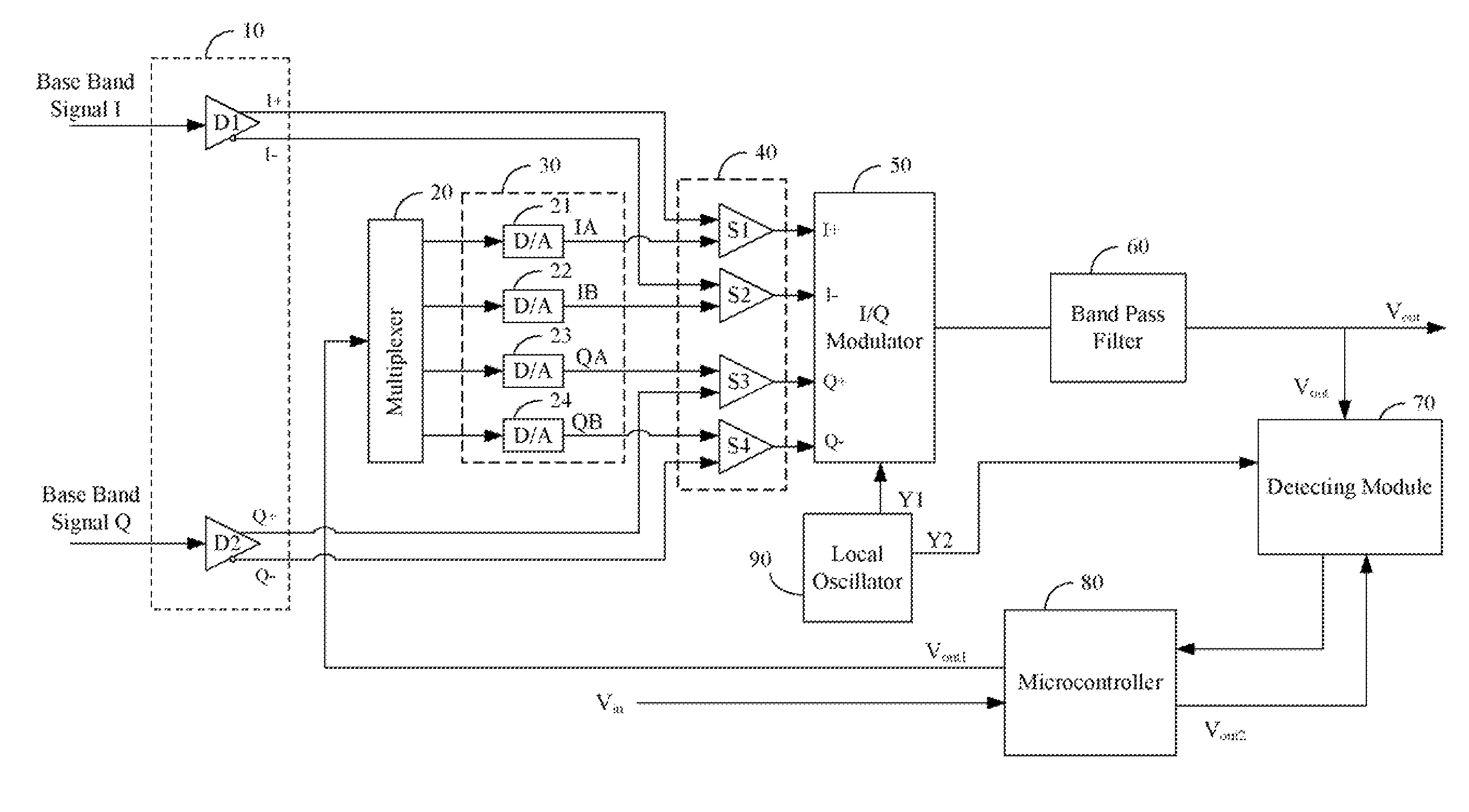
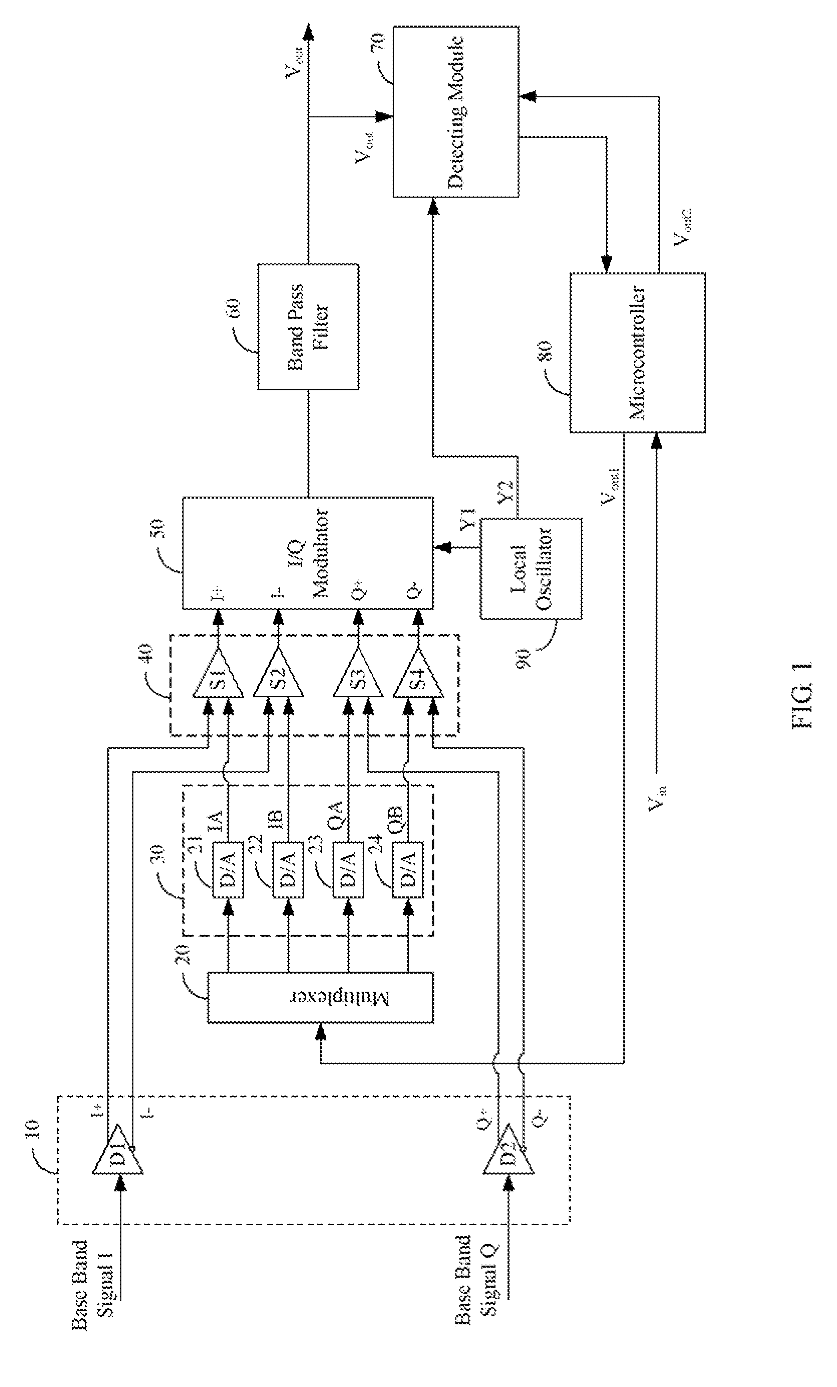
[0011]FIG. 1 is a block diagram of a circuit for canceling DC offset of an exemplary embodiment of the present invention. The circuit includes a differential amplifier assembly 10, a multiplexer 20, a digital-to-analog (D / A) converter assembly 30, a summing circuit 40, an inphase-to-quadrature (I / Q) modulator 50, a band pass filter 60, a detecting module 70, a microcontroller 80, and a local oscillator 90.

[0012]The differential amplifier assembly 10 converts a received base band signal to a differential base band signal. Normally, the base band signal includes vectors I and Q. In the exemplary embodiment, the differential amplifier assembly 10 includes two differential amplifiers D1 and D2, for receiving the vectors I and Q, and converting the vectors I and Q to differential vectors I+, I−, Q+, and Q−.

[0013]The D / A converter assembly 30 includes a plurality of D / A converters 21, 22, 23, and 24, which converts digital DC offset regulation signals to analog DC offset regulation signal...