Check patentability & draft patents in minutes with Patsnap Eureka AI!

Area array adapter

a technology of array adapter and array plate, which is applied in the direction of coupling device connection, sustainable manufacturing/processing, and final product manufacturing, etc., can solve the problems of different thermal expansion/contraction rate of solder and electrical components, increased stress on bga joints, and increased resistance of solder connections

Active Publication Date: 2010-10-05
HAMILTON SUNDSTRAND CORP
View PDF11 Cites 1 Cited by
  • Summary
  • Abstract
  • Description
  • Claims
  • Application Information

AI Technical Summary

Benefits of technology

The patent describes an adaptor that connects a component with a BGA connection type to a circuit board with a printed pad pattern using a Leaded Grid Array (LGA) connection type using electrical leads. This allows the BGA component to electrically connect to a LGA circuit board. The technical effect of this invention is the ability to connect components with different connection types on the same circuit board, improving the overall efficiency and reliability of electronic devices.

Problems solved by technology

One disadvantage of using a BGA joint type arises because the solder and the electrical component have different thermal expansion / contraction rates than the circuit board to which they are attached.
This difference results in stress placed on the BGA joints whenever there is thermal expansion or contraction.
Due to the nature of a BGA joint the solder connection is particularly susceptible to additional stresses resulting from thermal expansion and contraction.
The stress can cause a decrease in the lifespan of the joint and can lead to potential breakage.

Method used


Image

  • Area array adapter
  • Area array adapter

Examples


Embodiment Construction

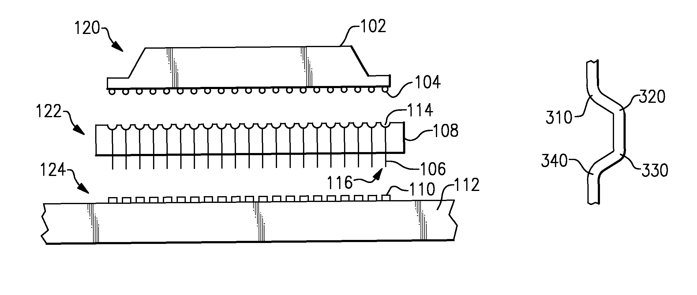
[0012]Referring to FIG. 1, an example apparatus having a BGA component 120, an area array adaptor 122, and a circuit board 124 is illustrated with an exploded view. In this example the BGA component 120 comprises an array of solder balls 104 on a bottom surface of a component operating portion 102. Each of the solder balls 104 in the array is capable of forming an electrical connection between the component operating portion 102 and another object, such as an adaptor 122.

[0013]The adaptor 122 shown in FIG. 1 is a cutout drawing providing a view of leads 106 located inside the area array adaptor 122. Each of the leads 106 is electrically conductive and corresponds to a connection needed for a BGA component 120 / circuit board 124 connection. Each of the leads 106 is held in a carrier material 108. The carrier material 108 is non-conductive, and, depending on the material's composition, can also provide a cushioning for thermal expansion and contraction of the circuit board 124, the ada...


PUM


Abstract

An adaptor for connecting ball grid array components to a circuit board with a leaded grid array joint, utilizing electric leads which can connect to a ball grid array on one end and a leaded grid array pad pattern on the opposite end.

Description

BACKGROUND OF THE INVENTION[0001]The present application is related to circuit board assemblies, and specifically to an adaptor for connecting an electrical component with a ball grid array joint to a circuit board with a leaded grid array joint.[0002]When creating circuit boards for performing specific functions a common method is to “print” electrical connections on the circuit board and then have joints where non-printable components (such as micro-chips, capacitors, etc.) can be connected to the printed board to complete the circuit. There are multiple standard joint types used to form these connections in the art.[0003]One type of joint is a Ball Grid Array (BGA) joint where the component has balls of solder at each connection which are joined with the board using a total heating method, which solders the component to the board.[0004]One disadvantage of using a BGA joint type arises because the solder and the electrical component have different thermal expansion / contraction rat...

Claims


Application Information

Patent Timeline
Patent Type & Authority Patents(United States)
IPC IPC(8): H01R12/00
CPCH01R12/57H01R13/2435H05K3/3426H05K7/1053H01R12/7082H01R13/2478H01R13/2485H01R13/41H05K2201/10734H05K2201/10946H01R12/716Y02P70/50
Inventor DESANTIS, CHARLES V.BURCHELL, DAVID E.
Owner HAMILTON SUNDSTRAND CORP
Features
  • R&D
  • Intellectual Property
  • Life Sciences
  • Materials
  • Tech Scout
  • Unparalleled Data Quality
  • Higher Quality Content
  • 60% Fewer Hallucinations
Learn More