Method and apparatus for buffering signals in voltage domains

a voltage domain and buffering technology, applied in electrical apparatus, pulse automatic control, solid-state devices, etc., can solve the problems of limiting the number of feed-through signals, limiting the number of buffers available in an integrated circuit, and not allowing the placement of standard cells

Inactive Publication Date: 2011-05-24
ATI TECH INC
View PDF6 Cites 20 Cited by
  • Summary
  • Abstract
  • Description
  • Claims
  • Application Information

AI Technical Summary

Problems solved by technology

Using the example of FIG. 1, this poses a problem because the second voltage domain 104 is capable of being selectively turned on and off.
However, prior art solutions either limited the location of buffers to specific locations and thereby fixed the number of available buffers in the second voltage domain 104 or required the use of or dependency upon at least one switching cell as discussed below.
Following these prior art methodologies was costly as it limited the locations where circuit designers placed buffers and resulted in limiting the number of feed-through signals that could be fed through and buffered in a second voltage domain like second voltage domain 104 of integrated circuit 100.
This solution, however, does not permit the placement of standard cells associated with the selectably on voltage supply grid VDD2 in the space and corresponding rows that have a pair of switching cells in columns 606.
Thus, this solution also limited the number of buffers available in an integrated circuit by the number of switching cells present and the number of buffers located in the space and corresponding row between pairs of switching cells.
The solution also wasted space by not permitting the placement of standard cells in the space and corresponding row between pairs of switching cells.

Method used


Image

  • Method and apparatus for buffering signals in voltage domains
  • Method and apparatus for buffering signals in voltage domains
  • Method and apparatus for buffering signals in voltage domains

Examples


Embodiment Construction

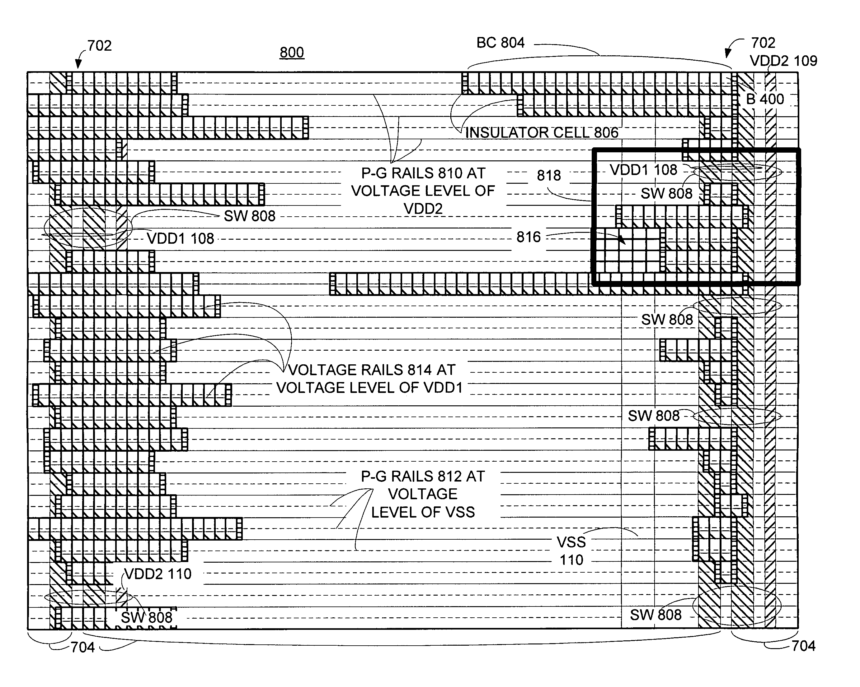
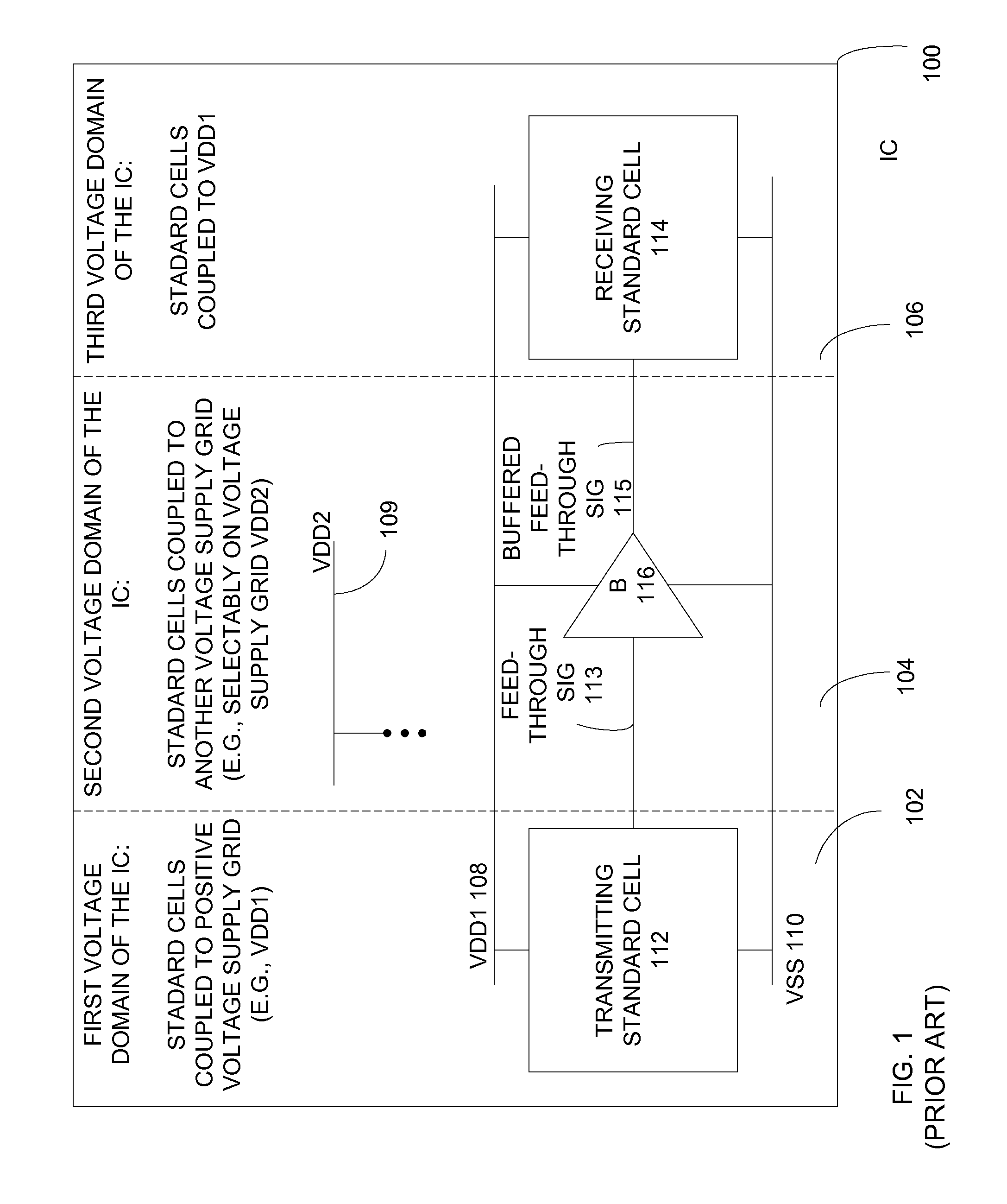
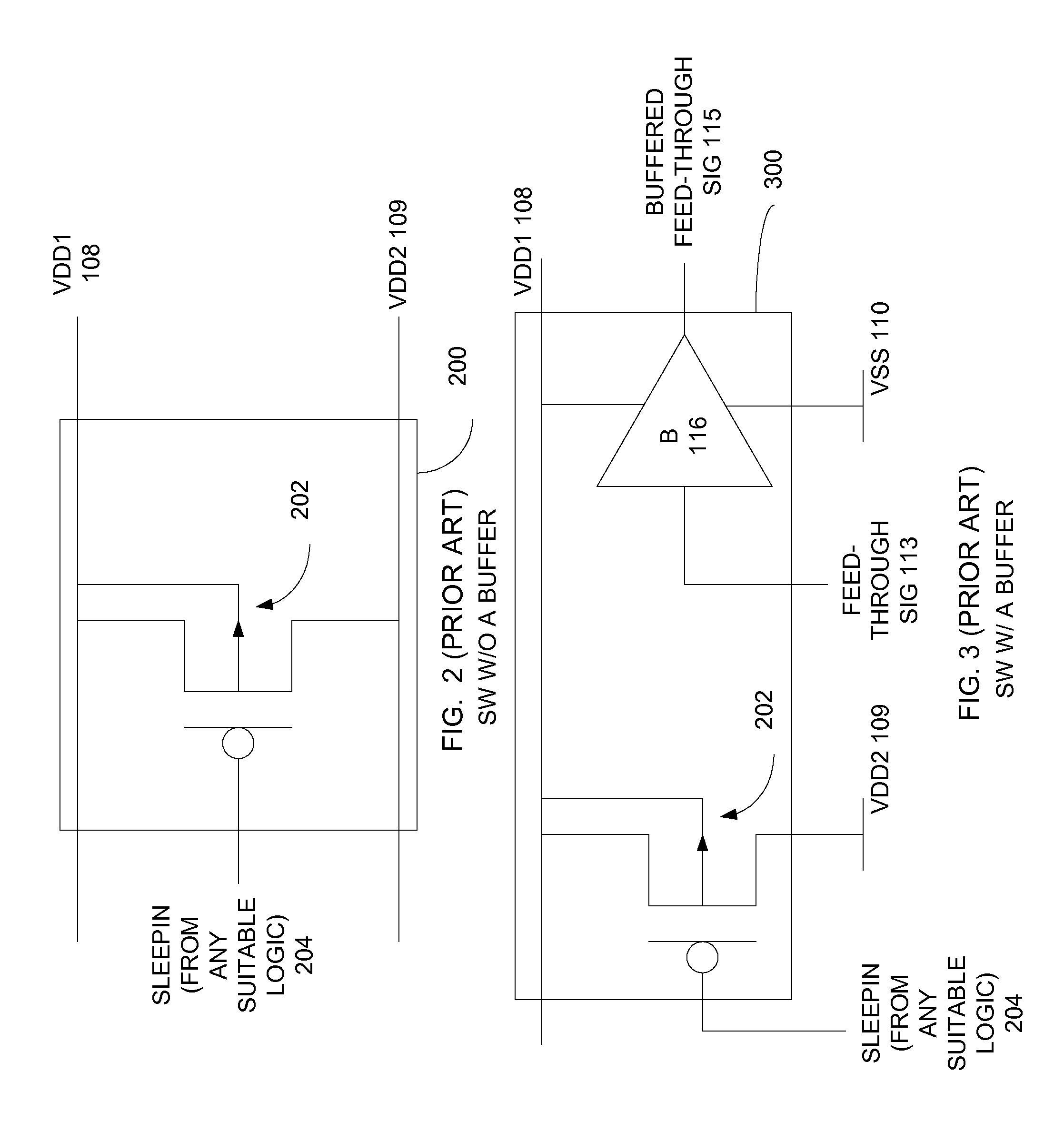
[0036]Generally, the present disclosure provides an integrated circuit and memory for designing an integrated circuit having buffer cells to improve buffering of feed-through signals in a voltage domain. The integrated circuit of the present disclosure includes at least first and second voltage domains. The first voltage domain is associated with a positive voltage supply grid while the second voltage domain is associated with a selectably on voltage supply grid. A switch having a first and second node is used to selectably switch on and off the selectably on voltage supply grid to power the second voltage domain. A buffer cell cluster of at least one initial buffer cell and a pair of insulator cells is coupled to the positive voltage supply grid and is electrically independent of the nodes of the switch and is capable of buffering a feed-through signal having a logic one voltage level defined substantially at the voltage level of the positive voltage supply grid. In one embodiment,...


PUM


Abstract

An integrated circuit includes first and second voltage domains. The first voltage domain is associated with a positive voltage supply grid and the second voltage domain is associated with a selectably on voltage supply grid. A switch is used to selectably switch on and off the selectably on voltage supply grid to power the second voltage domain. A buffer cell cluster of at least on initial buffer cell and a pair of insulator cells is coupled to the positive voltage supply grid electrically independent of the nodes of a switch and is capable of buffering a feed-through signal having a logic one voltage level defined substantially at the voltage level of the positive voltage supply grid. The buffer cell cluster has two distal ends. buffer cell cluster, at one distal end, is coupled to a first insulator cell of the pair of cells while, at the other distal end, the buffer cell cluster is coupled to a second insulator cell of the pair of the cells.

Description

CROSS-REFERENCE TO RELATED APPLICATION[0001]This application claims priority to the provisional patent application having Application No. 60 / 976,181, filed Sep. 28, 2007, having inventors Robert Chiu et al. and owned by instant assignee, for a METHOD AND APPARATUS FOR BUFFERING SIGNALS IN VOLTAGE DOMAINS.FIELD OF THE INVENTION[0002]The present disclosure generally relates to integrated circuits having more than one voltage domain and that are capable of buffering signals in the integrated circuit, and more particularly, to buffering signals in a voltage domain of an integrated circuit that is capable of being powered down independent of another voltage domain of the integrated circuit.BACKGROUND OF THE INVENTION[0003]As the explosion of electronic devices such as televisions, computers (i.e., anything that computes), monitors, mobile phones, personal digital assistants, handheld devices, etc. continue to push the technological envelope with respect to their ability to perform tasks ...

Claims


Application Information

Patent Timeline
Patent Type & Authority Patents(United States)
IPC IPC(8): H03L5/00
CPCH01L27/0207H03K19/0008H01L27/11898
Inventor CHIU, ROBERTTCHOEVSKA, DENITZANAJDESAMII, PARISSASTERNBERG, MARK H.
Owner ATI TECH INC
Why Eureka
Try Eureka