Electro-optical device and electronic apparatus

a technology of optical devices and electronic devices, applied in the direction of static indicating devices, non-linear optics, instruments, etc., can solve the problems of easy generation of voltage variation, display failure in the pixel region, and difficulty in arranging sampling switches in the arrangement direction of data lines in the peripheral region of the substrate, etc., to achieve high-quality color

Active Publication Date: 2012-09-18
SEIKO EPSON CORP
View PDF4 Cites 4 Cited by
  • Summary
  • Abstract
  • Description
  • Claims
  • Application Information

AI Technical Summary

Benefits of technology

[0008]An advantage of some aspects of the invention is that it provides an electro-optical device in which an adverse influence on the display due to a variation in voltage generated in data lines is unlikely to be viewed and a high-quality color image can be displayed, and an electronic apparatus including the electro-optical device.
[0014]Accordingly, the output lines of the green sampling switches (the lines led from the green sampling switches to the data lines in the peripheral region in order to electrically connect the green sampling switches arranged in the peripheral region and the data lines arranged in the pixel region) can be shorter than those of the plurality of red sampling switches and the plurality of blue sampling switches. Accordingly, among the output lines of the green sampling switches, the red sampling switches and the blue sampling switches, it is possible to minimize a variation in voltage due to capacitive coupling with other lines in the output lines of the green sampling switches. Accordingly, it is possible to suppress the variation in voltage in the green data lines corresponding to green having high visibility (or visual efficiency) of human. Even when the variation in voltage is generated in the red data lines and the blue data lines corresponding to red and blue, an adverse influence on the display is not substantially generated because red and blue have the visibility of human lower than that of green. As a result, it is possible to display high-quality color image.
[0019]By this configuration, the plurality of red sampling switches, the plurality of green sampling switches and the plurality of blue sampling switches are arranged so as to form one row in different directions and are arranged in three rows in one direction. Accordingly, each of the red sampling switches, the green sampling switches and the blue sampling switches are configured by a thin film transistor having a size larger than that of each of the sub pixels and can be readily arranged in the peripheral region.

Problems solved by technology

In such a color display liquid crystal device, since the sampling switches are provided in correspondence with the data lines corresponding to the sub pixels of R, G and B, it is difficult to arrange the sampling switches in a line in the arrangement direction of the data lines in the peripheral region of the substrate.
Accordingly, a variation in voltage is susceptible to be generated due to capacitive coupling with other lines in the output line of the sampling switch.
Accordingly, a display failure may occur in the pixel region by the variation in voltage of the image signal maintained in the data line electrically connected to the output line of the sampling switch.
Even when the variation in voltage is generated in the red data lines and the blue data lines corresponding to red and blue, an adverse influence on the display is not substantially generated because red and blue have the visibility of human lower than that of green.
Since blue has the visibility of human lower than that of red, it is difficult to view an adverse influence on the display due to the variation in voltage which may be generated in the data lines, compared with the case where the plurality of red sampling transistors are arranged further than the plurality of blue sampling transistors from the pixel region.

Method used


Image

  • Electro-optical device and electronic apparatus
  • Electro-optical device and electronic apparatus
  • Electro-optical device and electronic apparatus

Examples


first embodiment

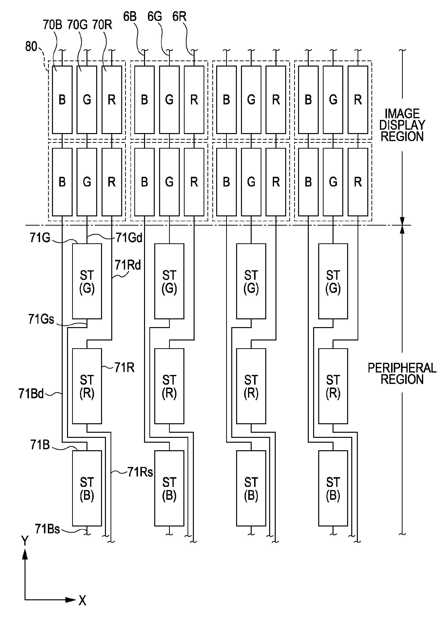
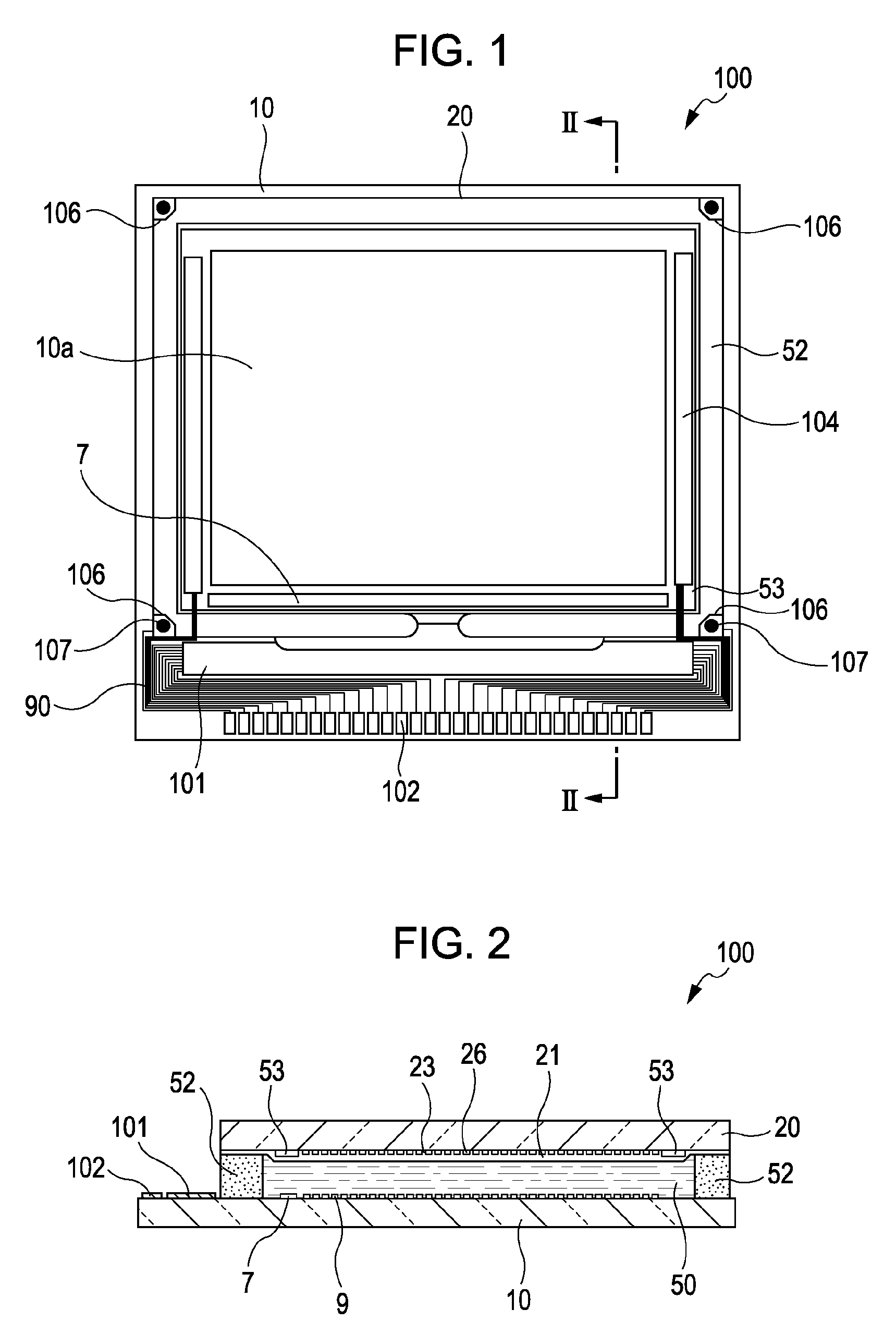
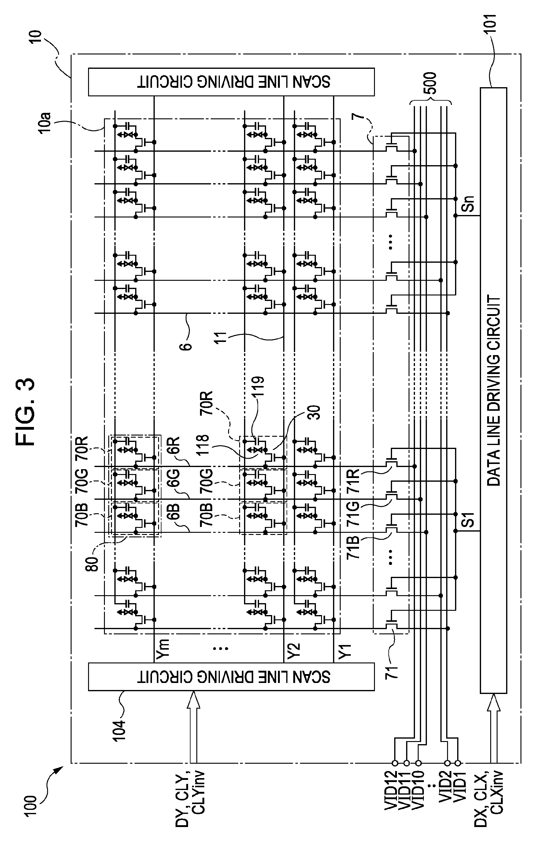
[0032]A liquid crystal device according to a first embodiment will be described with reference to FIGS. 1 to 5.

[0033]First, the whole configuration of the liquid crystal device according to the present embodiment will be described with reference to FIGS. 1 and 2. FIG. 1 is a plan view showing the configuration of a liquid crystal device according to the present embodiment. FIG. 2 is a cross-sectional view taken along line II-II of FIG. 1.

[0034]In FIGS. 1 and 2, in the liquid crystal device 100 of the present embodiment, a TFT array substrate 10 and a counter substrate 20 face each other. A liquid crystal layer 50 is interposed between the TFT array substrate 10 and the counter substrate 20. The TFT array substrate 10 and the counter substrate 20 are adhered to each other by a seal material 52 provided in a seal region located at the periphery of an image display region 10a as an example of a “pixel region” of the invention.

[0035]In FIG. 1, a frame light-shielding film 53 defining a ...


PUM

PropertyMeasurementUnit
wavelengthaaaaaaaaaa

Abstract

An electro-optical device includes red, green, and blue sub pixels and red, green, and blue data lines connected to the corresponding sub pixels. Red, green, and blue sampling switches are provided in a peripheral region and are electrically connected to data lines of the corresponding color. The green sampling switch is located at a position that is closer to the pixel region than are the red or blue sampling switches.

Description

BACKGROUND[0001]1. Technical Field[0002]The present invention relates to an electro-optical device such as a liquid crystal device and an electronic apparatus including the electro-optical device, such as a liquid projector.[0003]2. Related Art[0004]A liquid crystal device as an example of an electro-optical device is driven on the basis of an image signal supplied from an external circuit to an image signal line. The image signal is supplied from the image signal line to a plurality of data lines mounted in a pixel region of a substrate (that is, a region in which a plurality of pixels are, for example, arranged in a matrix) via a sampling circuit (for example, see Japanese Patent No. 3841074 and JP-A-2002-49331). The sampling circuit is provided in a peripheral region located on the periphery of the pixel region and includes a plurality of sampling switches respectively provided in the data lines. Each of the sampling switches is constituted by a one-channel type or complementary ...

Claims


Application Information

Patent Timeline
Patent Type & Authority Patents(United States)
IPC IPC(8): G09G3/36G02F1/1345
CPCG02F1/136286G02F1/1345G09G3/3688G09G2310/0297G02F1/133
Inventor MASUI, JUNICHI
Owner SEIKO EPSON CORP
Why Eureka
Try Eureka