Power conversion device
- Summary
- Abstract
- Description
- Claims
- Application Information
AI Technical Summary
Benefits of technology
Problems solved by technology
Method used
Image
Examples
first embodiment
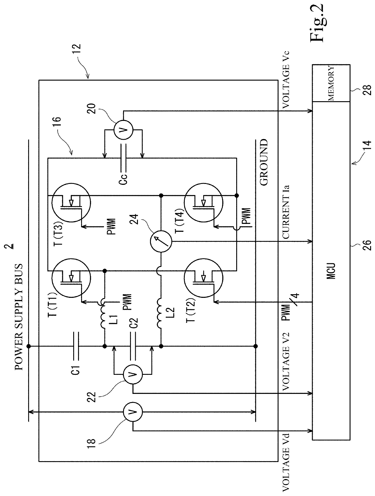
[0043]FIG. 2 is a circuit diagram showing the power conversion device 2 according to an embodiment of the present invention. As shown in the figure, the device 2 includes a variation compensation circuit 12 and a control circuit 14.
[0044]The variation compensation circuit 12 is connected to a power supply bus. As shown in FIG. 2, the variation compensation circuit 12 includes a first capacitor C1, a second capacitor C2, an auxiliary capacitor Cc, a converter 16, a first voltmeter 18, a second voltmeter 20, a third voltmeter 22, and an ammeter 24.
[0045]The first capacitor C1 has one end connected to the power supply bus and the other end connected to the second capacitor C2. The second capacitor C2 is inserted in series between the first capacitor C1 and a ground. The converter 16 is connected to the second capacitor C2 and the auxiliary capacitor Cc. The converter 16 includes two input terminals and two output terminals. Each input terminal is connected to a corresponding one of the...
second embodiment
[0088]FIG. 6 is a block diagram showing a control circuit 42 of a power conversion device 40 according to another embodiment of the present invention. The device 40 includes a variation compensation circuit identical to the variation compensation circuit 12 of the power conversion device 2 of FIG. 2. As seen from FIG. 6, the control circuit 42 includes a notch filter 44 (NF 44), a variation component voltage extracting section 46 (vd extracting section 46), an all-pass filter 48 (APF 48), an instantaneous active / reactive power calculating section 50 (pq calculating section 50), a section 52 for determining instantaneous active power as an intermediate manipulated variable (Pp determining section 52), a section 54 for determining instantaneous reactive power as an intermediate manipulated variable (Qp determining section 54), a section 56 for calculating a converter output current (IA calculating section 56), a section 58 for determining a voltage of the second capacitor C2 as an int...
examples
[0129]A power conversion device as shown in FIG. 6 was produced. A DC voltage source and an inverter were prepared as a power supply system for evaluation. The inventive device was connected to a power supply bus interposed between the DC voltage source and the inverter. A simulation environment for the inventive device and the power supply system was also prepared. The specifications of the inventive device (APD device) and the power supply system are shown in Table 1. As shown in Table 1, the total capacitance of the capacitors used in the inventive device is not more than 50 μF.
TABLE 1Specifications for EvaluationItemValuePowerInverter output power1 kWsupplyInverter power factor1systemInverter output single-50 Hzphase AC frequencyDC power supply bus300 VvoltageAPD First capacitor C125.7 μFdeviceSecond capacitor C23.5 μFAuxiliary capacitor Cc18.8 μFInductors L1 + L2200 μHFET turn-on resistance50 mΩFET switching frequency100 kHz
[0130][Voltage Variation of Power Supply Bus]
[0131]A s...
PUM
 Abstract
Description
Claims
Application Information


