Memory device, memory system and memory control method

A technology of a memory system and a memory unit, which is applied in static memory, digital memory information, information storage, etc., and can solve the problems of increased floor area and difficult expansion of capacity

Inactive Publication Date: 2021-04-02
SONY SEMICON SOLUTIONS CORP
View PDF11 Cites 0 Cited by
  • Summary
  • Abstract
  • Description
  • Claims
  • Application Information

AI Technical Summary

Problems solved by technology

However, currently existing resistive variable memories utilizing access transistors result in an increase in footprint per unit cell
Therefore, expansion of capacity is not easy even in miniaturization using the same design rule compared to, for example, flash memory such as NAND type

Method used


Image

  • Memory device, memory system and memory control method
  • Memory device, memory system and memory control method
  • Memory device, memory system and memory control method

Examples


Embodiment Construction

[0053] Hereinafter, some embodiments of the present disclosure are described in detail with reference to the accompanying drawings. Note that descriptions are made in the following order.

[0054] 1. Example

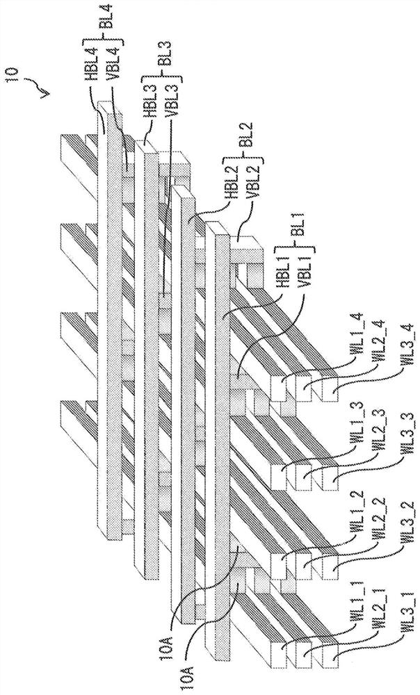
[0055] Examples including arrays of memory cells arranged in stacks ( Figure 1 to Figure 19 )

[0056] 2. Modification example

[0057] Modification A: Example where precharge is omitted ( Figure 21 to Figure 25 )

[0058] Modification B: Example of performing precharge when writing fails ( Figure 26 )

[0059] Modification C: Example of performing precharge according to the write position ( Figure 27 )

[0060] Modification D: Modification of the precharge circuit ( Figure 28 to Figure 30 )

[0061] Modification E: An example including a memory cell array in a single-layer arrangement ( Figure 31 and Figure 32 )

[0062] [1. Example]

[0063] [structure]

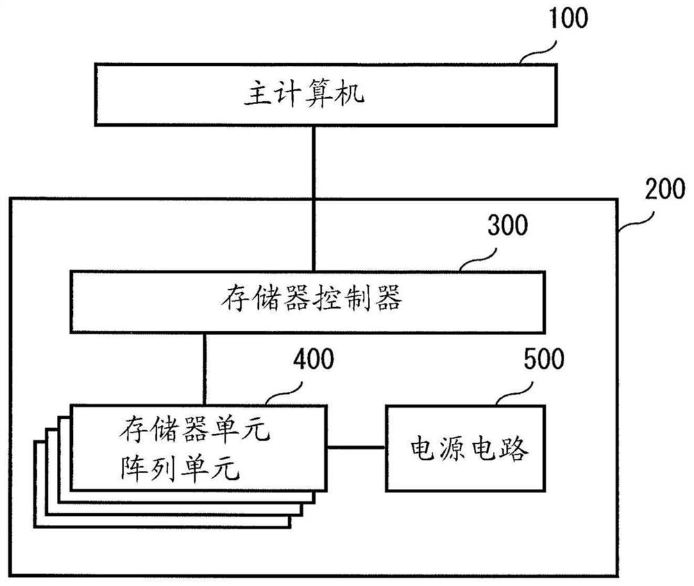
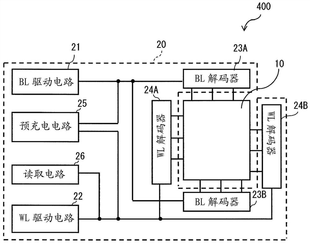
[0064] figure 1 One example of functional blocks of an information processing system accordi...


PUM


Abstract

A memory device according to an embodiment of the present technology includes: a plurality of memory cells arranged in a matrix; a plurality of row wirings connected to one end of each memory cell; a plurality of column wirings connected to the other end of each memory cell; A first decoder circuit connected to each row wiring of the even-numbered rows; a second decoder circuit connected to each of the row wirings of the odd-numbered rows; a third decoder circuit connected to each of the column wirings of the even-numbered columns; and Quad decoder circuit, connected to each column wire of odd columns. The first decoder circuit, the second decoder circuit, the third decoder circuit, and the fourth decoder circuit are composed of mutually independent circuits.

Description

technical field [0001] The present disclosure relates to a memory device including a decoder circuit, a memory system including the memory device, and a memory control method in the above-mentioned memory device. Background technique [0002] In recent years, there has been a desire to expand the capacity for data storage of nonvolatile memories typified by resistance variable memories such as ReRAM (Resistive Random Access Memory). However, currently existing resistance variable memories utilizing access transistors result in an increase in footprint per unit cell. Therefore, expansion of capacity is not easy even in miniaturization using the same design rule, compared with, for example, a flash memory such as a NAND type. Meanwhile, in the case of using a so-called cross-point array structure, the footprint per unit cell becomes smaller, leading to the realization of capacity expansion. A cross-point array structure includes an arrangement of memory elements at intersect...

Claims


Application Information

Patent Timeline
Patent Type & Authority Patents(China)
IPC IPC(8): G11C13/00
CPCG11C8/10G11C13/0023G11C13/0033G11C13/004G11C13/0061G11C13/0069G11C13/0026G11C13/0028G11C2213/71G11C13/0038G11C13/00
Inventor 寺田晴彦森阳太郎北川真
Owner SONY SEMICON SOLUTIONS CORP
Why Eureka
Try Eureka