
Liquid crystal display device comprising periodically changed permutations of at least two types of electrode-pattern pairs

a liquid crystal display device and electrode pattern technology, applied in non-linear optics, instruments, optics, etc., can solve the problems of large labor and cost, difficult to eliminate periodicity of surface irregularities completely, and large expenditure of labor and cost to randomize mask patterns, so as to prevent moiré patterns and effectively prevent light interference

Active Publication Date: 2013-02-05
NEC LCD TECH CORP
View PDF18 Cites 6 Cited by
  • Summary
  • Abstract
  • Description
  • Claims
  • Application Information

AI Technical Summary

Benefits of technology

[0047]An exemplary object of the present invention is to provide a liquid crystal display device which is capable of effectively preventing a moiré pattern from being produced due to the periods between an irregularity pattern on a reflecting plate surface and an electrode pattern in a pixel and also of effectively preventing the interference of light (iridescent light) reflected from a reflecting plate or electrodes in a reflective area.

Problems solved by technology

Generally, the vertical-electric-field liquid crystal display device has poorer viewing angle characteristics than the horizontal-electric-field liquid crystal display device.
Though it is ideal to randomize such surface irregularities, since the surface irregularities need to cover the surface uniformly two-dimensionally for uniformizing the reflected light, it is difficult to eliminate the periodicity of the surface irregularities completely.
In addition, it requires a large expenditure of labor and cost to randomize a mask pattern for a photomask in order to expose a photosensitive organic film.
It is not practical to randomize the surface irregularities of the reflecting film unlimitedly beyond one pixel.
However, even if the technology disclosed in Patent document 4 is applied to the pixel structure disclosed in Patent document 3, a moiré pattern is produced, lowering the quality of the displayed image, for the following reasons:
Particularly, the pixels disclosed in Patent document 4 are difficult to design for use as pixels for displaying high-definition images because the number of pixel electrodes that are disposed in one pixel is limited.
However, the displayed image suffered a moiré pattern and had a reduced quality for the reasons described below.
Moreover, if the electrodes are arranged with the above angle being increased, the proportion of the pixel aperture is reduced, resulting in a reduction in the performance of the display device.
Particularly with respect to high-definition display devices, since the size of pixels is small, the number of electrodes and reflecting surface irregularities that can be placed in a pixel are limited, tending to make the electrode pitch and the surface irregularity pitch substantially equal to each other.

Method used


Image

  • Liquid crystal display device comprising periodically changed permutations of at least two types of electrode-pattern pairs
  • Liquid crystal display device comprising periodically changed permutations of at least two types of electrode-pattern pairs
  • Liquid crystal display device comprising periodically changed permutations of at least two types of electrode-pattern pairs

Examples


first exemplary embodiment

3rd Aspect of First Exemplary Embodiment

[0240]A liquid crystal display device according to a third aspect of the first exemplary embodiment of the present invention will be described below. Only those details of the liquid crystal display device according to the third aspect of the first exemplary embodiment which are different from those of the liquid crystal display device according to the second aspect of the first exemplary embodiment will be described below.

[0241]FIG. 13 shows a plan view of a pixel of the liquid crystal display device according to the third aspect of the first exemplary embodiment. As shown in FIG. 13, the pixel has no transmissive area, but only has reflective area 5. Except for the above structure, the pixel has the same arrayed and combined pattern of electrode pairs as with the second aspect.

[0242]Since the structure according to the third aspect has a high reflectance, the liquid crystal display device according to the third aspect has high visibility in ...

second exemplary embodiment

4th Aspect of Second Exemplary Embodiment

[0267]A liquid crystal display device according to a fourth aspect of the second exemplary embodiment of the present invention will be described below. The liquid crystal display device according to the fourth aspect of the second exemplary embodiment is the same as the liquid crystal display device according to the first aspect of the first exemplary embodiment except for the electrode structure in the pixels. Only those details of the liquid crystal display device according to the fourth aspect of the second exemplary embodiment which are different from those of the liquid crystal display device according to the first aspect of the first exemplary embodiment will be described below.

[0268]FIG. 19 shows a plan view of the liquid crystal display device according to the fourth aspect of the second exemplary embodiment. As shown in FIG. 19, all electrodes disposed in reflective area 5 are disposed in the same layer. Pixel electrodes 27b and comm...

third exemplary embodiment

2nd Aspect of Third Exemplary Embodiment

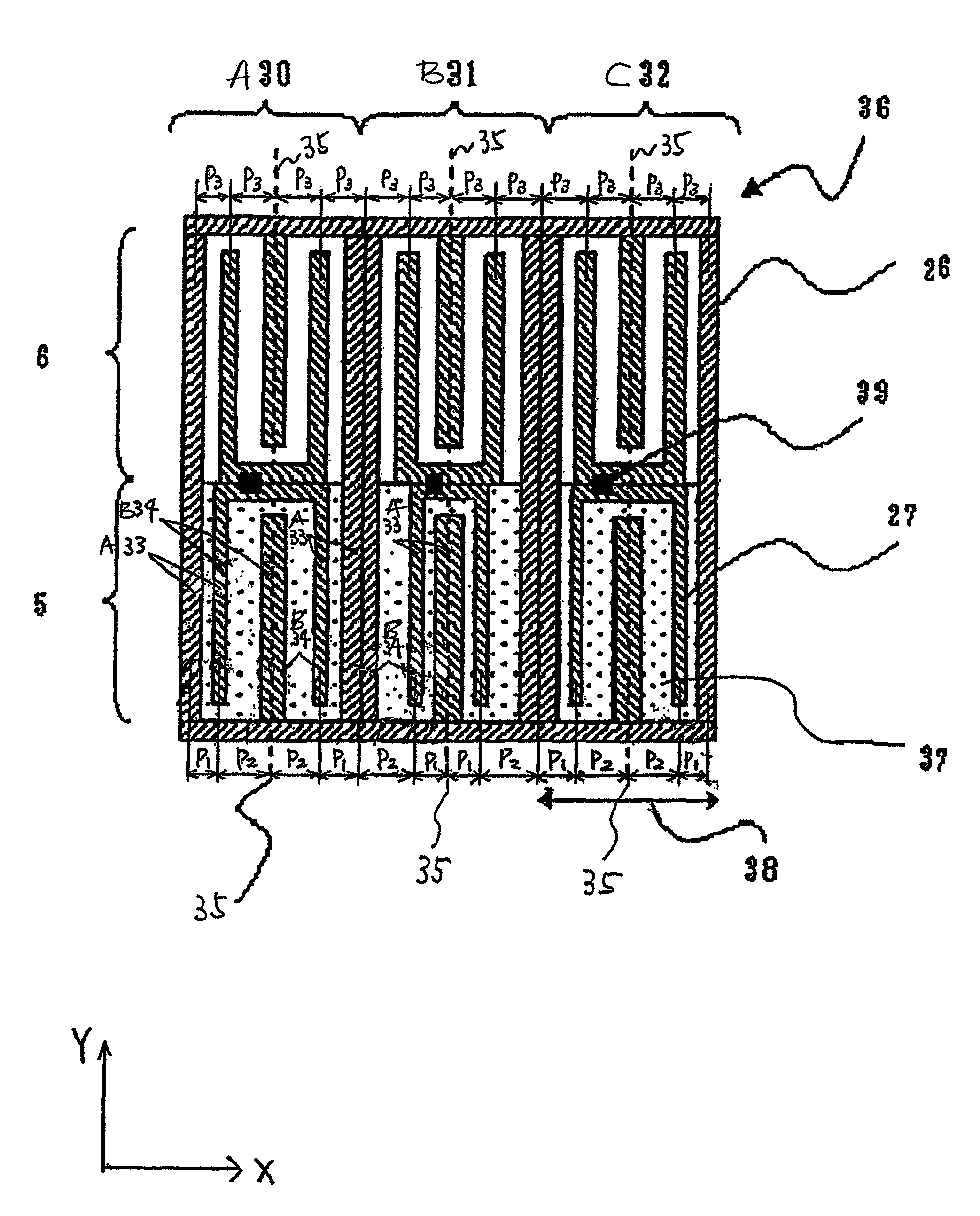
[0279]A liquid crystal display device according to a second aspect of the third exemplary embodiment of the present invention will be described below. The liquid crystal display device according to the second aspect of the third exemplary embodiment is the same as the liquid crystal display device according to the first aspect of the first exemplary embodiment except for the electrode structure in the pixels. Only those details of the liquid crystal display device according to the second aspect of the third exemplary embodiment which are different from those of the liquid crystal display device according to the first aspect of the first exemplary embodiment will be described below.

[0280]FIGS. 21(a) through 21(c) show a plan view of pixels of the liquid crystal display device according to the second aspect of the third exemplary embodiment. As shown in FIGS. 21(a) through 21(c), a pixel is divided into three dots 30, 31, 32 arrayed in the X-axi...


PUM

PropertyMeasurementUnit
angleaaaaaaaaaa
sizeaaaaaaaaaa
distanceaaaaaaaaaa

Abstract

A liquid crystal display device comprises a plurality of pixels arrayed in a first direction and a second direction, each of the pixels having a reflective area in at least a portion thereof. The reflective area comprises a surface-irregularity film that is a film having a plurality of surface irregularities, a light reflecting film disposed as an upper layer over the surface-irregularity film, and an electrode group disposed as an upper layer over the light reflecting film. The electrode group in each of the pixels that are arrayed in at least the first direction comprises at least two types of electrode patterns having different layouts.

Description

[0001]This application is based upon and claims the benefit of priority from Japanese patent application No. 2007-249281, filed on Sep. 26, 2007, the disclosure of which is incorporated herein in its entirety by reference.BACKGROUND OF THE INVENTION[0002]1. Field of the Invention[0003]The present invention relates to a semitransmissive or reflective electrooptical device having substrates with an electrooptical material held thereby, and an electronic device incorporating such a semitransmissive or reflective electrooptical device. In particular, the present invention is concerned with an IPS (In Plane Switching)-mode active-matrix liquid crystal display device.[0004]The term “semitransmissive liquid crystal display device” referred to herein means a display device having a reflective display area for reflecting incident light from an external source to display an image and a transmissive display area for transmitting light from a light source disposed behind to display an image.[00...

Claims


Application Information

Patent Timeline
Patent Type & Authority Patents(United States)
IPC IPC(8): G02F1/1335G02F1/1343
CPCG02F1/133555G02F1/134363G02F1/133553
Inventor NIIOKA, SHINYASUMIYOSHI, KEN
Owner NEC LCD TECH CORP
Learn More