Three-dimensional semiconductor memory devices and methods of fabricating the same

a semiconductor memory and three-dimensional technology, applied in the field of three-dimensional (3d) semiconductor memory devices, can solve the problems of fine patterning technology cost and practical limitation of planar semiconductor devices in high density

Active Publication Date: 2014-10-28
SAMSUNG ELECTRONICS CO LTD
View PDF28 Cites 27 Cited by
  • Summary
  • Abstract
  • Description
  • Claims
  • Application Information

AI Technical Summary

Problems solved by technology

However, the costs of such fine patterning technology set a practical limitation on integration of planar semiconductor devices in high density.

Method used


Image

  • Three-dimensional semiconductor memory devices and methods of fabricating the same
  • Three-dimensional semiconductor memory devices and methods of fabricating the same
  • Three-dimensional semiconductor memory devices and methods of fabricating the same

Examples


Embodiment Construction

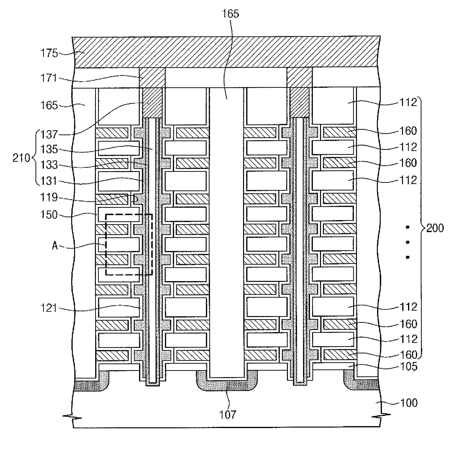
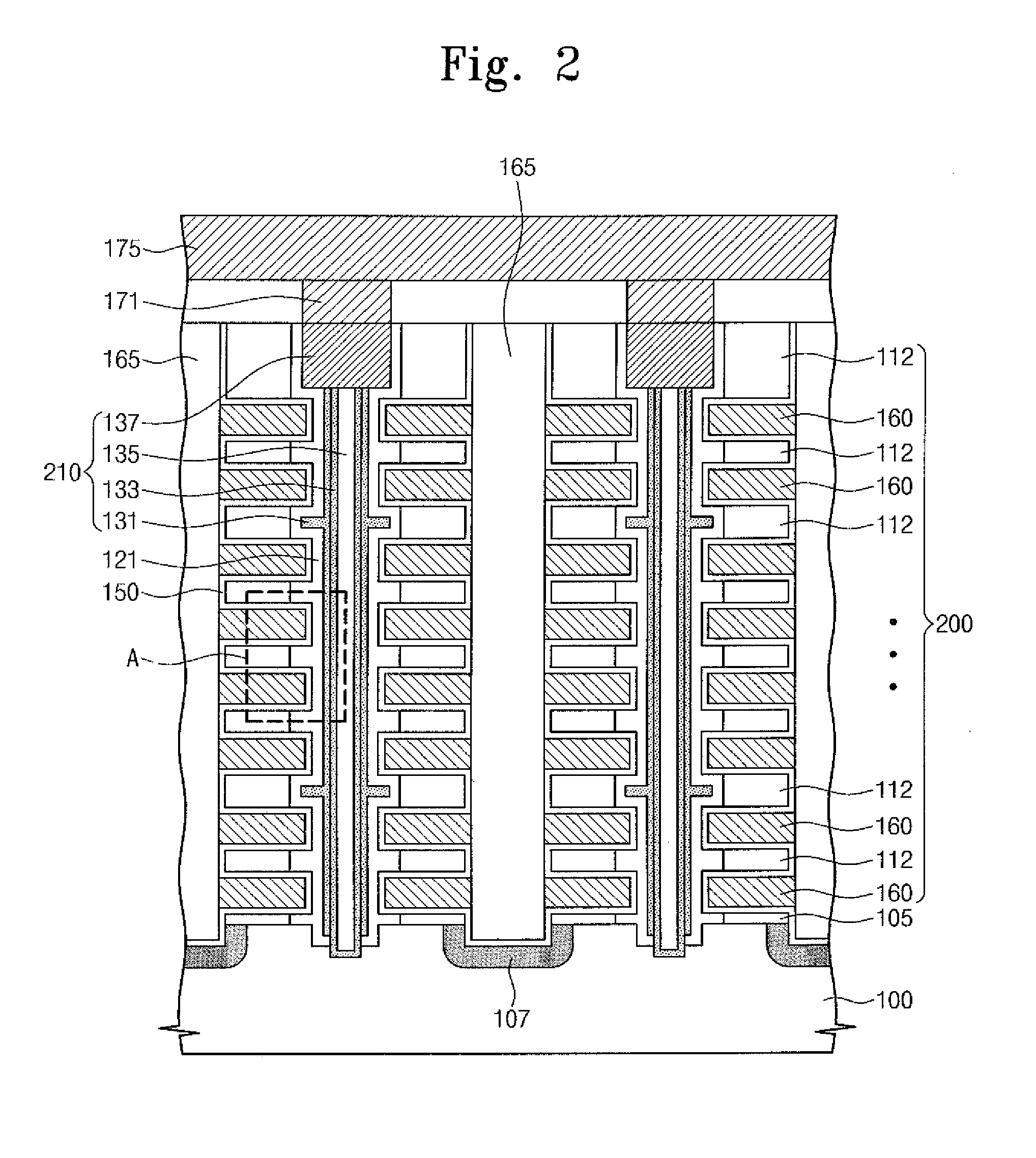
[0024]Exemplary embodiments of the inventive concept will be described below in more detail with reference to the accompanying drawings. However, the inventive concept may be embodied in different forms and should not be construed as limited to the embodiments set forth herein. Rather, these exemplary embodiments are provided so that this disclosure will be thorough and complete and will fully convey the inventive concept to those skilled in the art. In the drawings, the thickness of layers and regions may be exaggerated for clarity. Like reference numerals may refer to the like elements throughout the specification and drawings.

[0025]Hereinafter, 3D semiconductor memory devices and methods of fabricating the same according to an exemplary embodiment of the inventive concept will be described with reference to the drawings in more detail.

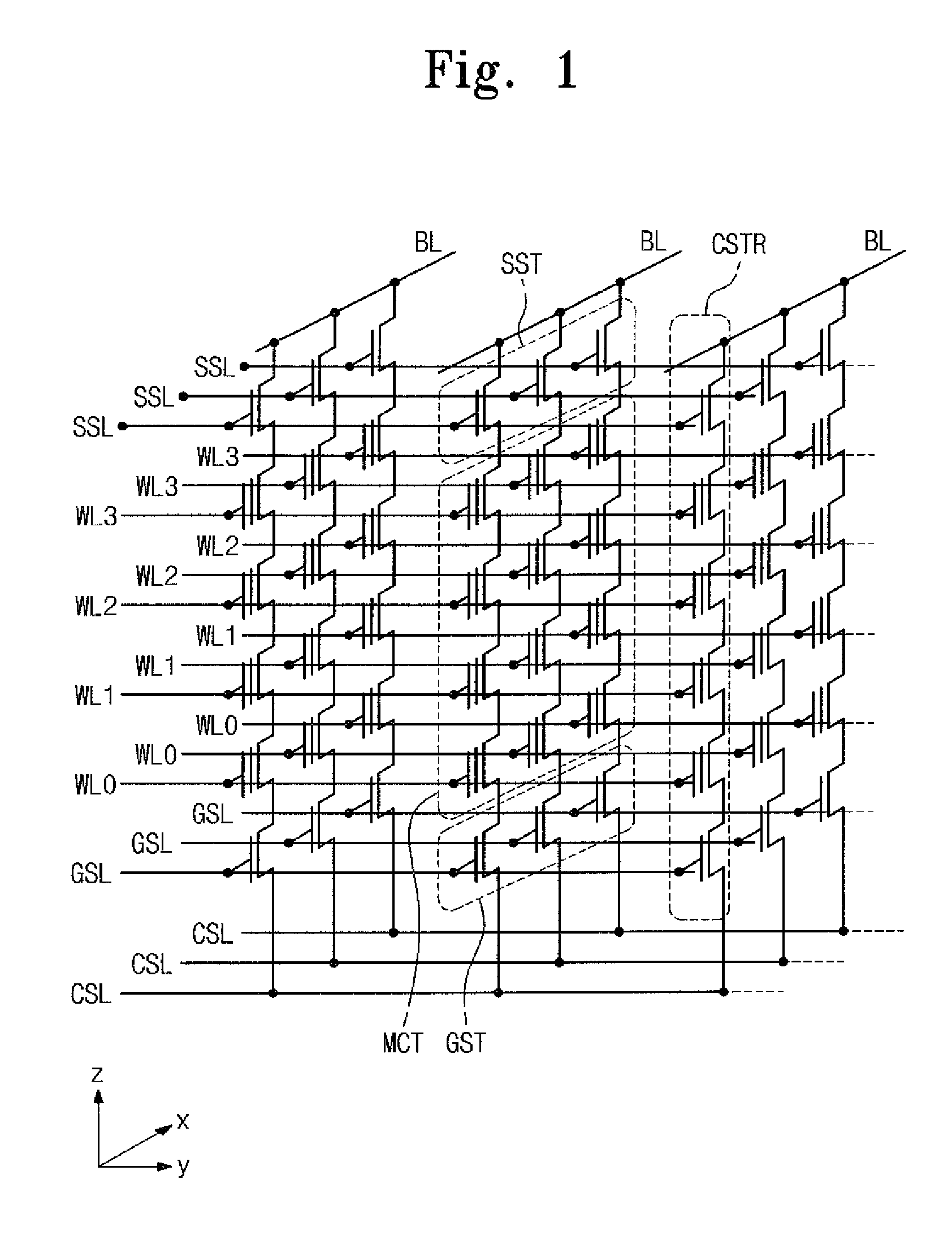
[0026]FIG. 1 is a schematic circuit diagram illustrating a three dimensional (3D) semiconductor memory device according to an exemplary embodiment ...


PUM


Abstract

A three-dimensional (3D) semiconductor memory device includes an electrode separation pattern, a stack structure, a data storage layer, and a channel structure. The electrode separation pattern is disposed on a substrate. A stack structure is disposed on a sidewall of the electrode separation pattern. The stack structure includes a corrugated sidewall opposite to the sidewall of the electrode separation pattern. The sidewall of the electrode separation pattern is vertical to the substrate. A data storage layer is disposed on the corrugated sidewall. A channel structure is disposed on the charge storage layer.

Description

CROSS-REFERENCE TO RELATED APPLICATION[0001]This application claims priority under 35 U.S.C. §119 to Korean Patent Application No. 10-2012-0039151, filed on Apr. 16, 2012, in the Korean Intellectual Property Office, the disclosure of which is incorporated by reference herein in its entirety.TECHNICAL FIELD[0002]The inventive concept relates to semiconductor devices and methods of fabricating the same and, more particularly, to three-dimensional (3D) semiconductor memory devices and methods of fabricating the same.DESCRIPTION OF THE RELATED ART[0003]Semiconductor devices have been highly integrated to provide consumers high end electronic device at an affordable price. A degree of integration has been an important factor in determining product prices, so high integration processes are desired in light of costs. For planar semiconductor memory devices, a degree of integration is primarily determined by a unit memory cell size. Accordingly, such degree of integration is greatly influen...

Claims


Application Information

Patent Timeline
Patent Type & Authority Patents(United States)
IPC IPC(8): H01L27/105
CPCH01L27/1052H01L29/7926H01L27/11582H10B43/27H01L21/823487H01L27/0688H10B99/00
Inventor LEE, JUYULKIM, BUMSUPARK, KWANGMINPARK, HYUNAHN, JAE-YOUNGYOO, DONGCHULCHUN, JONGSIKHWANG, KIHYUN
Owner SAMSUNG ELECTRONICS CO LTD
Why Eureka
Try Eureka