Method of spacer patterning to form a target integrated circuit pattern

a technology of integrated circuit and spacer, which is applied in the direction of semiconductor/solid-state device manufacturing, basic electric elements, electric devices, etc., can solve the problems of scaling down and increasing the complexity of processing and manufacturing ics

Active Publication Date: 2017-02-21
TAIWAN SEMICON MFG CO LTD
View PDF6 Cites 1620 Cited by
  • Summary
  • Abstract
  • Description
  • Claims
  • Application Information

AI Technical Summary

Benefits of technology

[0037]In one exemplary aspect, the present disclosure is directed to a method of forming a target pattern for an integrated circuit (IC). The method includes forming a plurality of lines over a substrate with a first mask; forming a first spacer layer over the substrate, over the plurality of lines, and onto sidewalls of the plurality of lines; removing at least a portion of the first spacer layer to expose the plurality of lines; removing the plurality of lines thereby providing a patterned first spacer layer over the substrate; forming a second spacer layer over the substrate, over the patterned first spacer layer, and onto sidewalls of the patterned first spacer layer; and forming a patterned material layer over the second spacer layer with a second mask thereby the patterned material layer and the second spacer layer collectively define a plurality of trenches.

Problems solved by technology

Such scaling down has also increased the complexity of processing and manufacturing ICs and, for these advances to be realized, similar developments in IC processing and manufacturing are needed.

Method used


Image

  • Method of spacer patterning to form a target integrated circuit pattern
  • Method of spacer patterning to form a target integrated circuit pattern
  • Method of spacer patterning to form a target integrated circuit pattern

Examples


Embodiment Construction

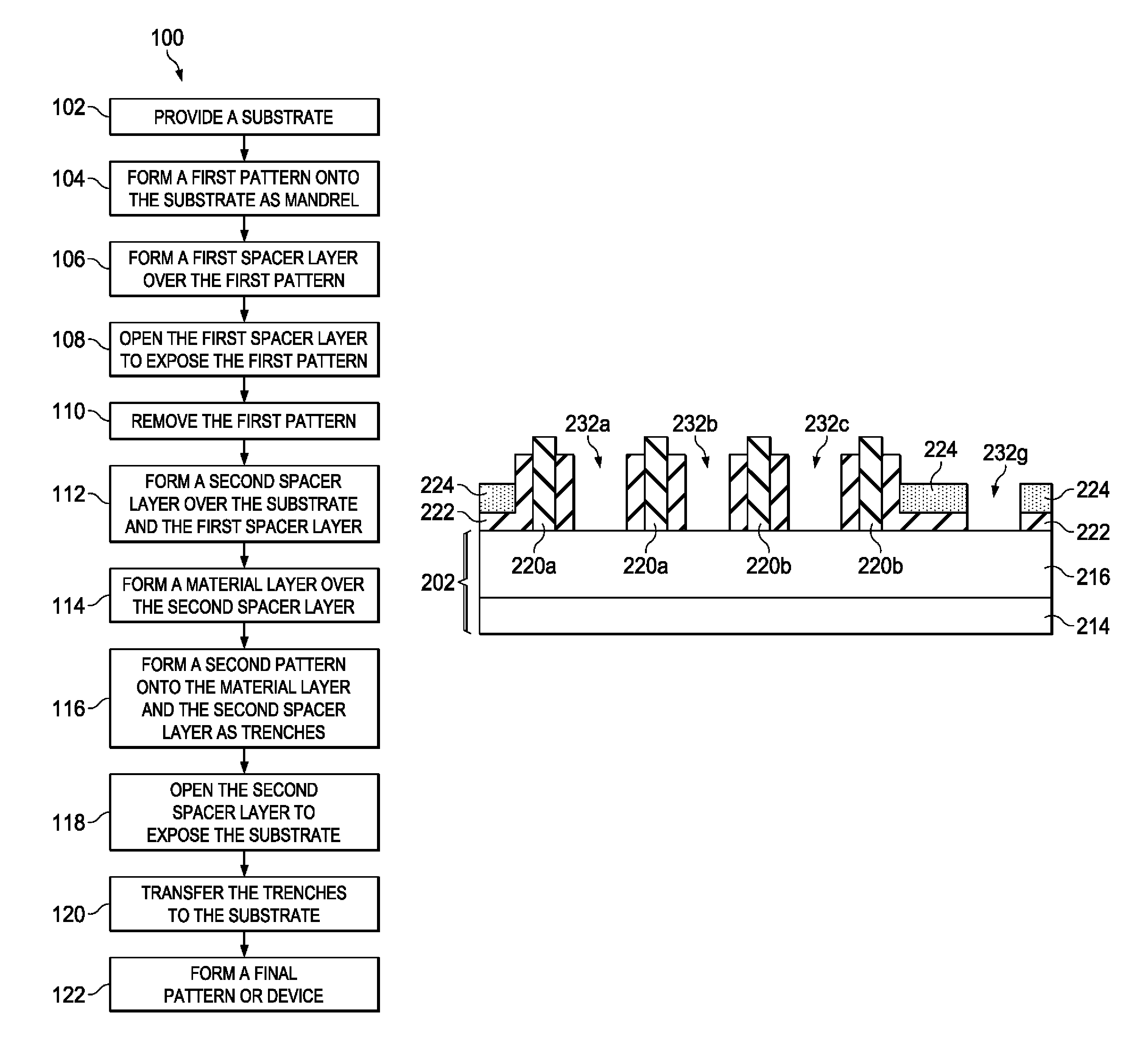
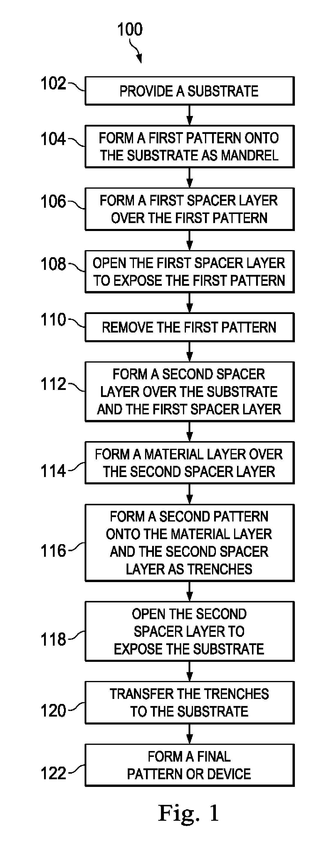
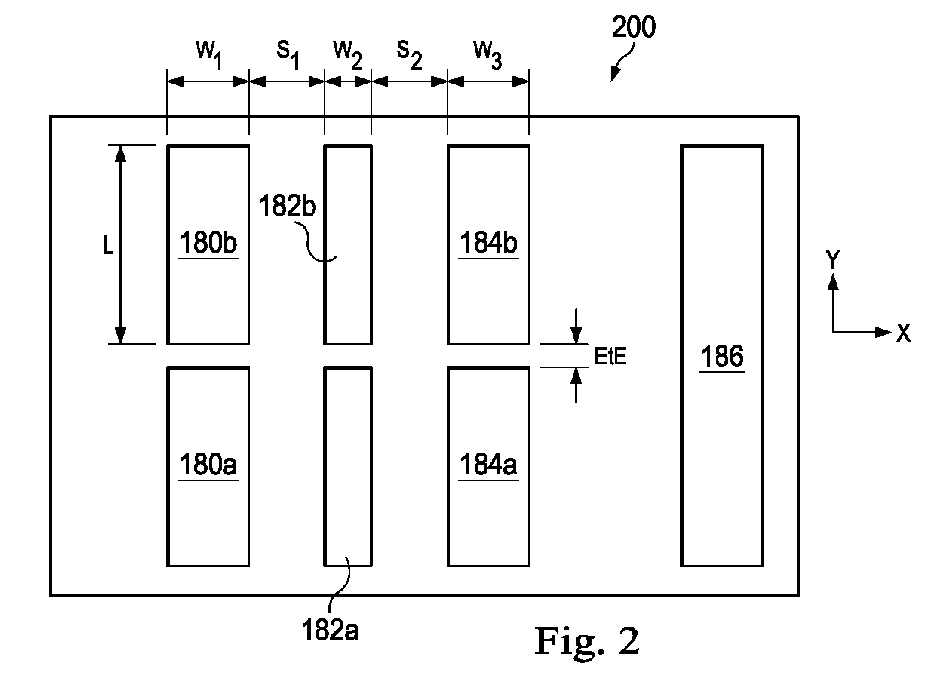
[0010]The following disclosure provides many different embodiments, or examples, for implementing different features of the disclosure. Specific examples of components and arrangements are described below to simplify the present disclosure. These are, of course, merely examples and are not intended to be limiting. In addition, the present disclosure may repeat reference numerals and / or letters in the various examples. This repetition is for the purpose of simplicity and clarity and does not in itself dictate a relationship between the various embodiments and / or configurations discussed. Moreover, the performance of a first process before a second process in the description that follows may include embodiments in which the second process is performed immediately after the first process, and may also include embodiments in which additional processes may be performed between the first and second processes. Various features may be arbitrarily drawn in different scales for the sake of si...


PUM


Abstract

A method of forming a target pattern includes forming a plurality of lines over a substrate with a first mask and forming a first spacer layer over the substrate, over the plurality of lines, and onto sidewalls of the plurality of lines. The plurality of lines is removed, thereby providing a patterned first spacer layer over the substrate. The method further includes forming a second spacer layer over the substrate, over the patterned first spacer layer, and onto sidewalls of the patterned first spacer layer, and forming a patterned material layer over the second spacer layer with a second mask. Whereby, the patterned material layer and the second spacer layer collectively define a plurality of trenches.

Description

PRIORITY DATA[0001]The present application is a continuation patent application of U.S. patent application Ser. No. 14 / 134,027, filed on Dec. 19, 2013, now U.S. Pat. No. 9,136,106, the disclosure of which is hereby incorporated by reference in its entirety.BACKGROUND[0002]The semiconductor integrated circuit (IC) industry has experienced exponential growth. Technological advances in IC materials and design have produced generations of ICs where each generation has smaller and more complex circuits than the previous generation. In the course of IC evolution, functional density (i.e., the number of interconnected devices per chip area) has generally increased while geometry size (i.e., the smallest component (or line) that can be created using a fabrication process) has decreased. This scaling down process generally provides benefits by increasing production efficiency and lowering associated costs. Such scaling down has also increased the complexity of processing and manufacturing IC...

Claims


Application Information

Patent Timeline
Patent Type & Authority Patents(United States)
IPC IPC(8): H01L21/308H01L21/768H01L21/02H01L21/033H01L21/027H01L21/306H01L21/311
CPCH01L21/3086H01L21/0274H01L21/02104H01L21/0337H01L21/308H01L21/30604H01L21/31116H01L21/76802H01L21/76816H01L21/0332H01L21/31111H01L21/31144
Inventor WU, CHIEH-HANTSAI, CHENG-HSIUNGLEE, CHUNG-JUSHIEH, MING-FENGLIU, RU-GUNSHUE, SHAU-LINBAO, TIEN-I
Owner TAIWAN SEMICON MFG CO LTD
Why Eureka
Try Eureka