Color filter substrate used in a display and its manufacturing method
a technology of color filter substrate and which is applied in the direction of photomechanical equipment, photosensitive material processing, instruments, etc., can solve the problems of increased material cost, extended period, low liquid crystal performance, etc., and achieves improved productivity, reduced production cost of liquid crystal display panel, and improved liquid crystal performance
- Summary
- Abstract
- Description
- Claims
- Application Information
AI Technical Summary
Benefits of technology
Problems solved by technology
Method used
Image


Examples
first embodiment
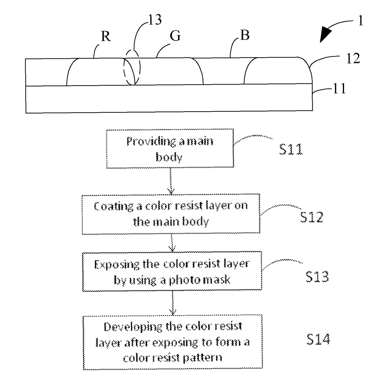
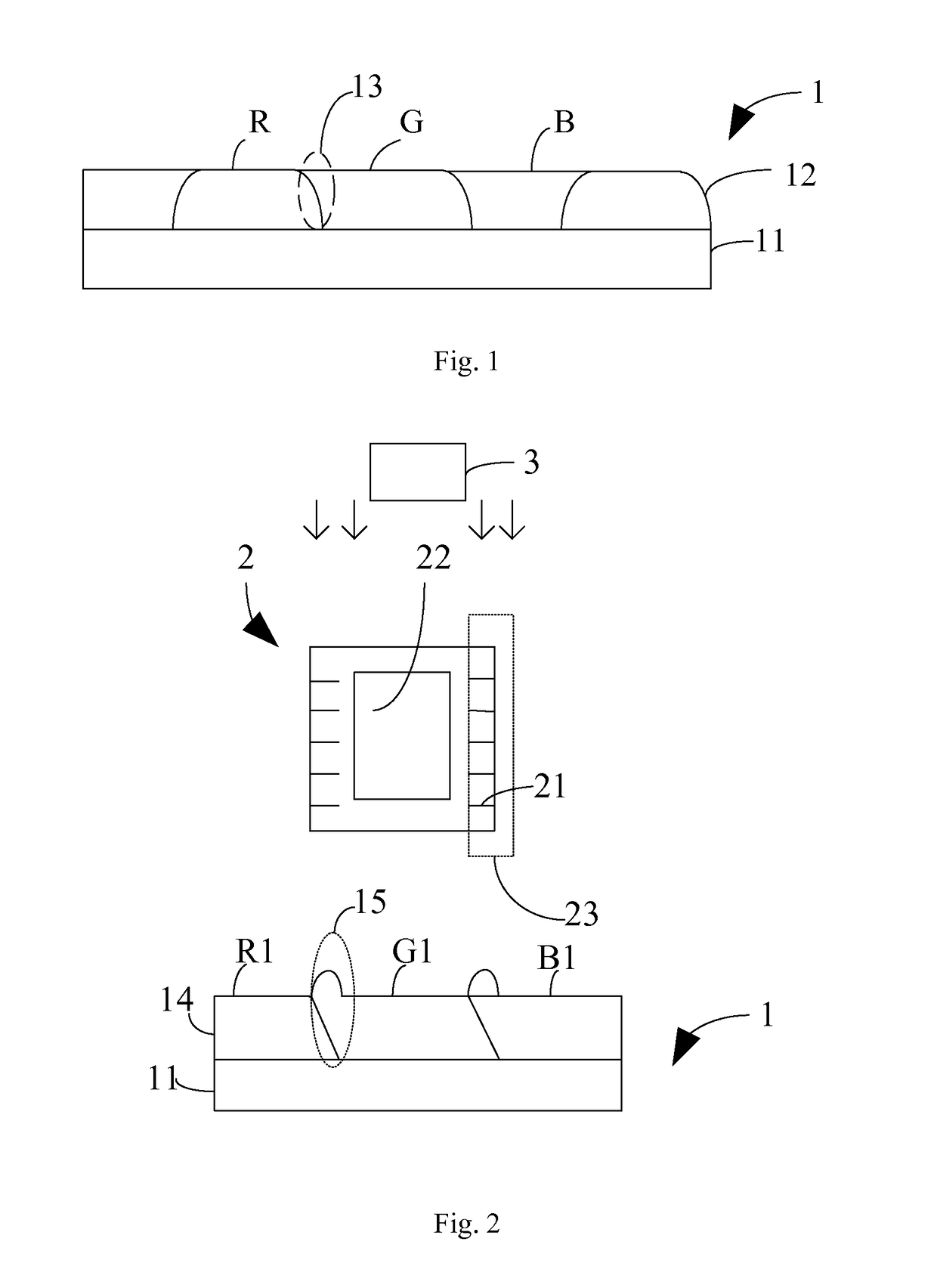
[0029]S13: Exposing the color resist layer 14 by using a photo mask 2, where the photo mask 2 of a color filter substrate 1 is shown in FIG. 4. FIG. 4 is a schematic structural diagram showing a photo mask of a color filter substrate based on the present invention. Please refer to FIG. 4. The photo mask 2 comprises a light shielding region 21 and a transmission area 22 surrounded by the light shielding region 21. A spaced shading pattern is disposed in an edge of the light shielding region 21 near the transmission region 22 to form a semi-transparent gray scale mask area 23, where the gray scale mask area 23 is disposed at the opposite sides of the light shielding region 21. The shape of the shading pattern is rectangle, triangle, trapezoid or semicircular. Otherwise, the shading pattern can further be other regular or irregular morphology such as a zigzagged shape, an arc shape or a trapezoidal shape to achieve the semi-transparent characteristic by using the patterning process in ...
second embodiment
[0030]Otherwise, the structure of the photo mask 2 of the color filter substrate 1 is shown in FIG. 5. FIG. 5 is a schematic structural diagram showing a photo mask of a color filter substrate based on the present invention, where similar with the photo mask 2 in FIG. 4, the photo mask 4 also comprise a light shielding region 41 and a transmission region 42 surrounded by the light shielding region 41. A spaced shading pattern is disposed in an edge of the light shielding region 41 near the transmission region 42 to form a semi-transparent gray scale mask area 43. The shading pattern is a rectangular shape, a triangular shape, a trapezoidal shape or a semicircular shape. FIG. 5 is the example of a rectangular shape for the present invention. Comparing with the photo mask 2 of FIG. 4, the gray scale mask area 43 of the photo mask 4 is disposed at the surrounding area of the light shielding region 41. It should be emphasized that no matter what the gray scale mask area 43 disposed at t...
PUM
| Property | Measurement | Unit |
|---|---|---|
| thickness | aaaaa | aaaaa |
| semi-transparent | aaaaa | aaaaa |
| color | aaaaa | aaaaa |
Abstract
Description
Claims
Application Information
 - R&D
- Intellectual Property
- Life Sciences
- Materials
- Tech Scout
- Unparalleled Data Quality
- Higher Quality Content
- 60% Fewer Hallucinations
Browse by: Latest US Patents, China's latest patents, Technical Efficacy Thesaurus, Application Domain, Technology Topic, Popular Technical Reports.
© 2025 PatSnap. All rights reserved.Legal|Privacy policy|Modern Slavery Act Transparency Statement|Sitemap|About US| Contact US: help@patsnap.com