Supercharge Your Innovation With Domain-Expert AI Agents!

Semiconductor device and method for fabricating the same

a semiconductor and gate capacitance technology, applied in the direction of semiconductor devices, basic electric elements, electrical equipment, etc., can solve the problems of reducing the gate capacitance, affecting the driving force of the device, and affecting the performance of the devi

Active Publication Date: 2017-09-12
UNITED MICROELECTRONICS CORP
View PDF14 Cites 1 Cited by
  • Summary
  • Abstract
  • Description
  • Claims
  • Application Information

AI Technical Summary

Benefits of technology

This approach protects the high-k dielectric layer and bottom barrier metal from etching gas, maintaining device performance by ensuring the structural integrity of the gate structure and preventing unwanted etching during spacer formation.

Problems solved by technology

However, the conventional polysilicon gate also faced problems such as inferior performance due to boron penetration and unavoidable depletion effect which increases equivalent thickness of gate dielectric layer, reduces gate capacitance, and worsens driving force of the devices.
However, in current fabrication of high-k metal transistor, particularly during the stage when spacer is formed on the sidewall of gate structure, issues such as over-etching or undercut often arise and causing etching gas to etch through spacer until reaching the bottom of the gate structure.
This induces erosion in high-k dielectric layer and / or bottom barrier metal (BBM) and affects the performance of the device substantially.

Method used


Image

  • Semiconductor device and method for fabricating the same
  • Semiconductor device and method for fabricating the same
  • Semiconductor device and method for fabricating the same

Examples


Embodiment Construction

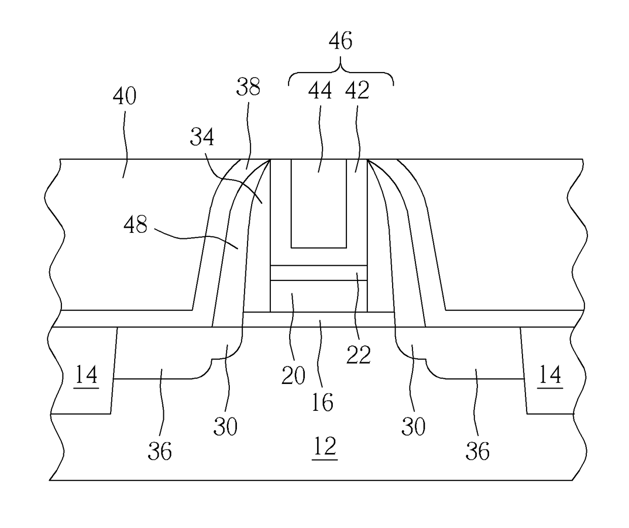
[0011]Referring to FIGS. 1-5, FIGS. 1-5 illustrate a method for fabricating semiconductor device according to a preferred embodiment of the present invention. As shown in FIG. 1, a substrate 12, such as a wafer or silicon-on-insulator (SOI) substrate is provided, in which a plurality of shallow trench isolations (STIs) 14 are formed in the substrate 12. An interfacial layer 16 is then deposited on the substrate 12 and the STI 14, and a stack structure 18 is formed on the substrate 12 thereafter. The formation of the stack structure 18 is accomplished by sequentially forming a high-k dielectric layer 20, a bottom barrier metal (BBM) layer 22, a silicon layer 24, and a hard mask 26 on the interfacial layer 16.

[0012]In this embodiment, the interfacial layer 16 is preferably composed of silicon material such as silicon dioxide (SiO2), silicon nitride (SiN), or silicon oxynitride (SiON), or other dielectric material with high permittivity or dielectric constant. The silicon layer 24 is p...


PUM

PropertyMeasurementUnit
dielectric constantaaaaaaaaaa
work functionaaaaaaaaaa

Abstract

A method for fabricating semiconductor device is disclosed. The method includes the steps of: providing a substrate; forming an interfacial layer on the substrate; forming a stack structure on the interfacial layer; patterning the stack structure to form a gate structure on the interfacial layer; forming a liner on the interfacial layer and the gate structure; and removing part of the liner and part of the interfacial layer for forming a spacer.

Description

BACKGROUND OF THE INVENTION[0001]1. Field of the Invention[0002]The invention relates to a method for fabricating semiconductor device, and more particularly, to a method of retaining interfacial layer while a stacked structure is patterned to form gate structure.[0003]2. Description of the Prior Art[0004]In current semiconductor industry, polysilicon has been widely used as a gap-filling material for fabricating gate electrode of metal-oxide-semiconductor (MOS) transistors. However, the conventional polysilicon gate also faced problems such as inferior performance due to boron penetration and unavoidable depletion effect which increases equivalent thickness of gate dielectric layer, reduces gate capacitance, and worsens driving force of the devices. In replacing polysilicon gates, work function metals have been developed to serve as a control electrode working in conjunction with high-K gate dielectric layers.[0005]However, in current fabrication of high-k metal transistor, particu...

Claims


Application Information

Patent Timeline
Patent Type & Authority Patents(United States)
IPC IPC(8): H01L29/66H01L29/49H01L29/51H01L29/78
CPCH01L29/66545H01L29/513H01L29/6656H01L29/7833H01L29/4966H01L29/401H01L29/511H01L29/517H01L29/518
Inventor HSU, CHIA-FUCHIOU, CHUN-MAOHSU, SHIH-CHIEHKUO, LUNG-ENJHANG, YOU-DIKE, JIAN-CUN
Owner UNITED MICROELECTRONICS CORP
Features
  • R&D
  • Intellectual Property
  • Life Sciences
  • Materials
  • Tech Scout
  • Unparalleled Data Quality
  • Higher Quality Content
  • 60% Fewer Hallucinations
Learn More