
A kind of preparation method of high-brightness flip-chip ultraviolet LED chip
A technology of LED chips and LED epitaxial wafers, applied in electrical components, circuits, semiconductor devices, etc., to reduce contact voltage, reduce absorption, and improve brightness
Patent Information
- Authority / Receiving Office
- CN · China
- Patent Type
- Patents(China)
- Current Assignee / Owner
- Publication Date
- 2017-02-15
- Estimated Expiration
- Not applicable · inactive patent
Smart Images
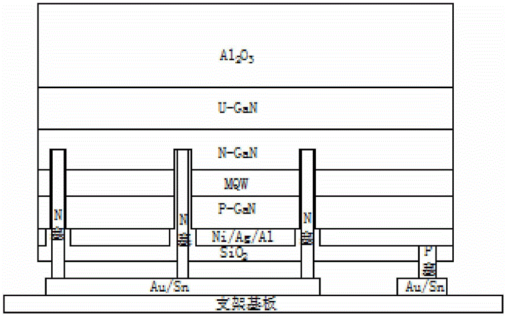
Figure 1 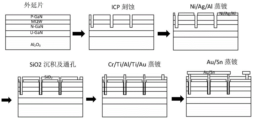
Figure 2
Abstract
Description
technical field
[0001] The invention belongs to the technical field of LED chip preparation, and mainly relates to a method for preparing a high-brightness flip-chip ultraviolet LED chip. Background technique
[0002] With the development of LED applications, UV LEDs are widely used because of their wider spectral range (light emitting wavelengths can cover the 210-400nm band), more energy-saving, and no toxic mercury. In many aspects of life, such as UV disinfection, UV hardening, optical sensors, UV authentication, body fluid detection and analysis and other fields. At present, the technical bottleneck of ultraviolet LED is mainly low efficiency. For chips with a wavelength lower than 365nm, the output power of the UV LED is only 5%-8% of the input power; when the wavelength is above 385nm, the efficiency of the UV LED is improved, but only 15% of the input power.
[0003] Flip-chip LED chips can effectively improve the brightness of LED chips. The traditional flip-chip...
Examples
Embodiment 1
[0029] figure 1 It is a structural diagram of a flip-chip ultraviolet LED chip of the present invention, and its manufacturing process is as follows figure 2 Shown: Using ICP etching technology for low-damage ultraviolet gallium nitride etching, using evaporation technology for high reflectivity P-type ohmic contact Ni / Ag / Al thin film preparation and P, N binding electrode Au / Sn film Layer preparation, using PECVD to deposit a silicon dioxide insulating layer and using BOE to etch it to form P and N electrode through holes.
[0030] The best embodiment of preparation technology is given below:
[0031] 1. Use aqua regia (HNO 3 : HCl=1:3) for surface treatment for 10 minutes, rinse with deionized water and dry;
[0032] 2. Put it into the ICP equipment for low-damage ultraviolet gallium nitride etching technology. The P-type gallium nitride layer and the underlying multi-quantum well light-emitting layer in the epitaxial wafer are etched to expose the N-type gallium nitride...
Embodiment 2
[0043] The thin film evaporation machine performs Ni / Ag thin film evaporation, and the Ni evaporation rate is Evaporation thickness The Ag evaporation rate is Evaporation thickness When evaporating, the vacuum degree is higher than 2.0×10⁻⁶Torr; the annealing temperature is 400°C, and the annealing time is 8 minutes; the thin film evaporation machine performs Al thin film evaporation, and the evaporation rate is Evaporation thickness The rest of the processes are the same as those in the first embodiment, and a high-brightness flip-chip ultraviolet LED chip can be prepared, which can be directly welded by eutectic soldering technology.
Embodiment 3
[0045] The thin film evaporation machine performs Ni / Ag thin film evaporation, and the Ni evaporation rate is Evaporation thickness The Ag evaporation rate is Evaporation thickness When evaporating, the vacuum degree is higher than 2.0×10⁻⁶Torr; nitrogen protection annealing, annealing temperature 410 ℃, annealing time 10min; thin film evaporation machine for Al thin film evaporation, evaporation rate is Evaporation thickness The rest of the processes are the same as those in the first embodiment, and a high-brightness flip-chip ultraviolet LED chip can be prepared, which can be directly welded by eutectic soldering technology.
[0046] 40*40mil prepared using the scheme of the present invention 2 The ultraviolet LED chip with a peak wavelength of 375nm has an optical power of 90mw and a voltage of 3.5V; the chip with a peak wavelength of 385nm has an optical power of 155mw and a voltage of 3.3V; the chip with a peak wavelength of 400nm has an optical power of 250mw ...