
Covalent functionalization of carbon nanotubes grown on a surface
a carbon nanotube and functionalization technology, applied in the field of covalent functionalization of carbon nanotubes grown on a surface, can solve the problems of large process errors, inability to functionalize cnts when on the chip, and problems such as reproducibility of devices, so as to reduce/eliminate facilitate the operation of nanostructures, and reduce the risk of short circui
Patent Information
- Authority / Receiving Office
- US · United States
- Patent Type
- Applications(United States)
- Current Assignee / Owner
- Publication Date
- 2022-05-19
Smart Images
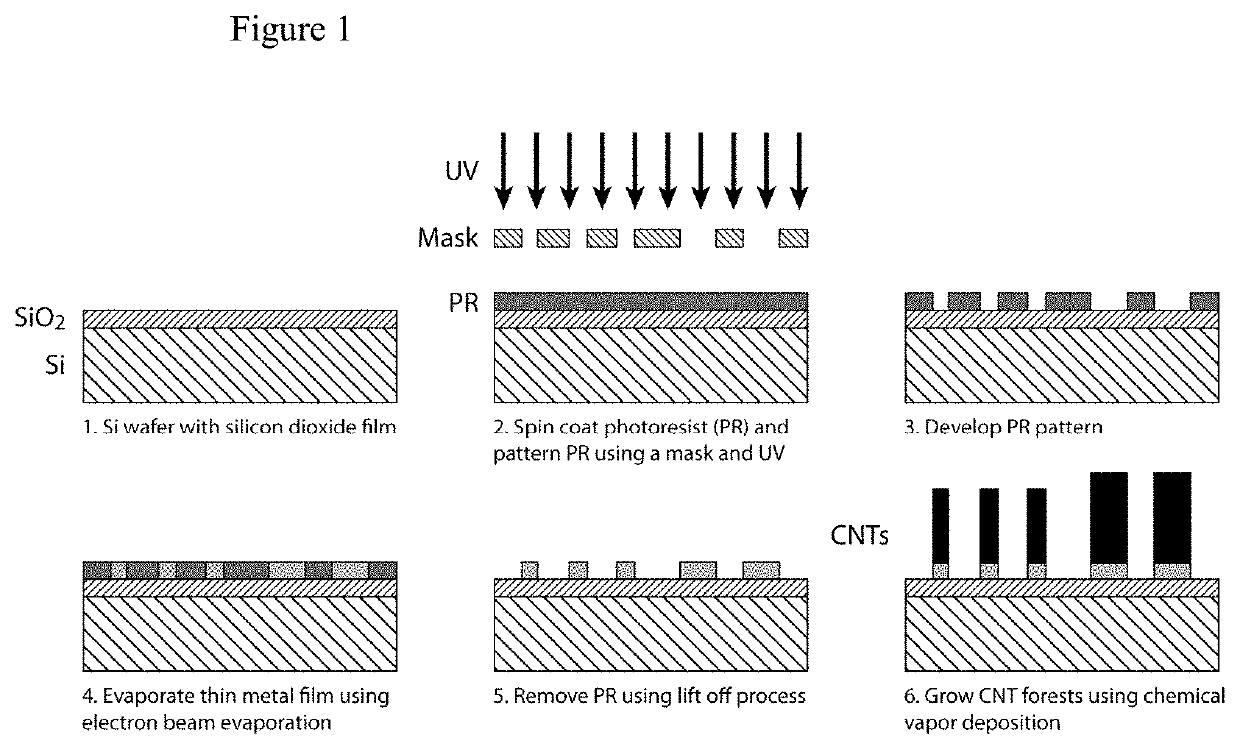
Figure 1 
Figure 2 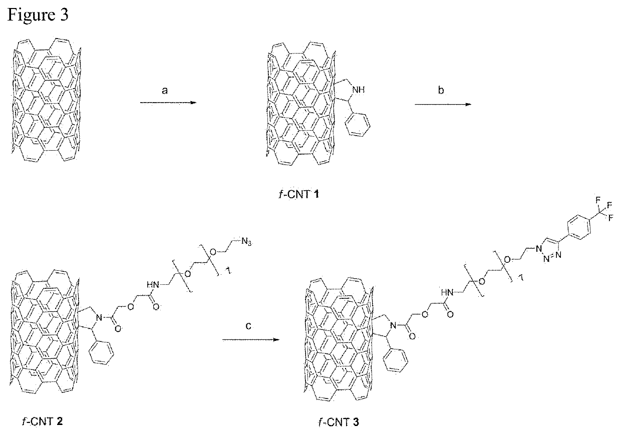
Figure 3
Abstract
Description
RELATED APPLICATIONS
[0001] This application is a continuation of International Application PCT / IB2013 / 000954, with an international filing date of Mar. 8, 2013, which claims priority to U.S. Application No. 61 / 609,011, filed on Mar. 9, 2012, the entire contents of which are incorporated by reference herein.FIELD OF THE INVENTION
[0002] The present invention is related to a new method for directly covalently functionalizing carbon nanotubes (CNTs) grown on or attached to a surface. The invention also features devices that are comprised of CNTs.BACKGROUND OF THE INVENTION
[0003] Carbon nanotubes (CNTs) possess unique properties such as small size and electrical conductivity, which makes them suitable in a wide range of potential applications, including use as structural materials in molecular electronics, nanoelectronic components, nanosensors and field emission displays. Carbon nanotubes may be either multi-walled (MWNTs) or single-walled (SWNTs), and have diameters in the nanometer range...
Examples
example 1
Fabrication of CNT Structures
[0117]The fabrication process for the CNT forest on chip is shown in FIG. 1.
[0118]A silicon wafer with a 0.5 μm silicon oxide was used as the substrate. Using lithography, a pattern was created on a photo resist (PR) film on the substrate. Electron beam evaporation was employed to deposit thin films of metals (Ti 1 nm / Mo 100 nm / Al2O3 5 nm / Fe 1 nm). Iron film is used as a catalyst to grow CNT forests. After e-beam evaporation, the photoresist is dissolved in an organic solvent (Photoresist remover) assisted by an ultrasonic bath, a process known as lift-off. The wafer is diced into chips and CNT forests are grown on the chips using thermal chemical vapor deposition (CVD) process. In this process, the catalyst (iron) is first annealed at 500° C. for 5 minutes in the presence of Hydrogen and Nitrogen. Later, ethylene, hydrogen and nitrogen gases are added at 700° C. and hence, CNT forests are grown by CVD. The process is carried out in a cold tube furnace s...
example 2
Functionalization Process
[0121]The strategy to functionalize CNT forests on chip is based on the well known 1,3-dipolar cycloaddition of azomethine yields to C60 and SWCNT in solution and is outlined in the scheme shown in FIG. 3. The azomethine ylide was formed upon heating to 120° C. in dichlorobenzene from the imine formed in situ between glycine and benzaldehyde, and reacted with CNT forests on chip. The procedure yielded the amine-modified CNT forest on chip, f-CNT 1, after cleaning. f-CNT 1 was further functionalized by an amide coupling with O-(2-azidoethyl)-O-[2-(diglycolyl-amino)ethyl]heptaethylene glycol to introduce azide functionalities on the CNT's. The amide coupling was carried out using PyBOP as coupling reagent under mild basic conditions (DIPEA in anhydrous CH2Cl2 at r.t.) to obtain azide functionalized CNT forests on chip, f-CNT 2. The functionalized CNT forests on chip were analyzed using SEM with EDS. To prove that f-CNT 2 were functionalized with azide groups, ...