

Input device, and electro-optical device
A technology of input device and electro-optical device, which is applied in the input/output process of data processing, electrical digital data processing, instruments, etc., can solve the problems of unusable, low degree of freedom, etc., and achieve the effect of high reliability
- Summary
- Abstract
- Description
- Claims
- Application Information
AI Technical Summary
Problems solved by technology
Method used
Image

Examples
no. 1 Embodiment approach
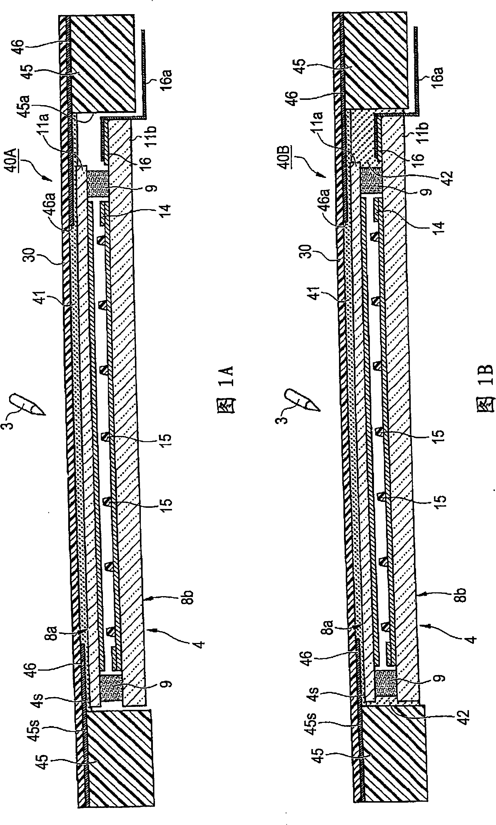
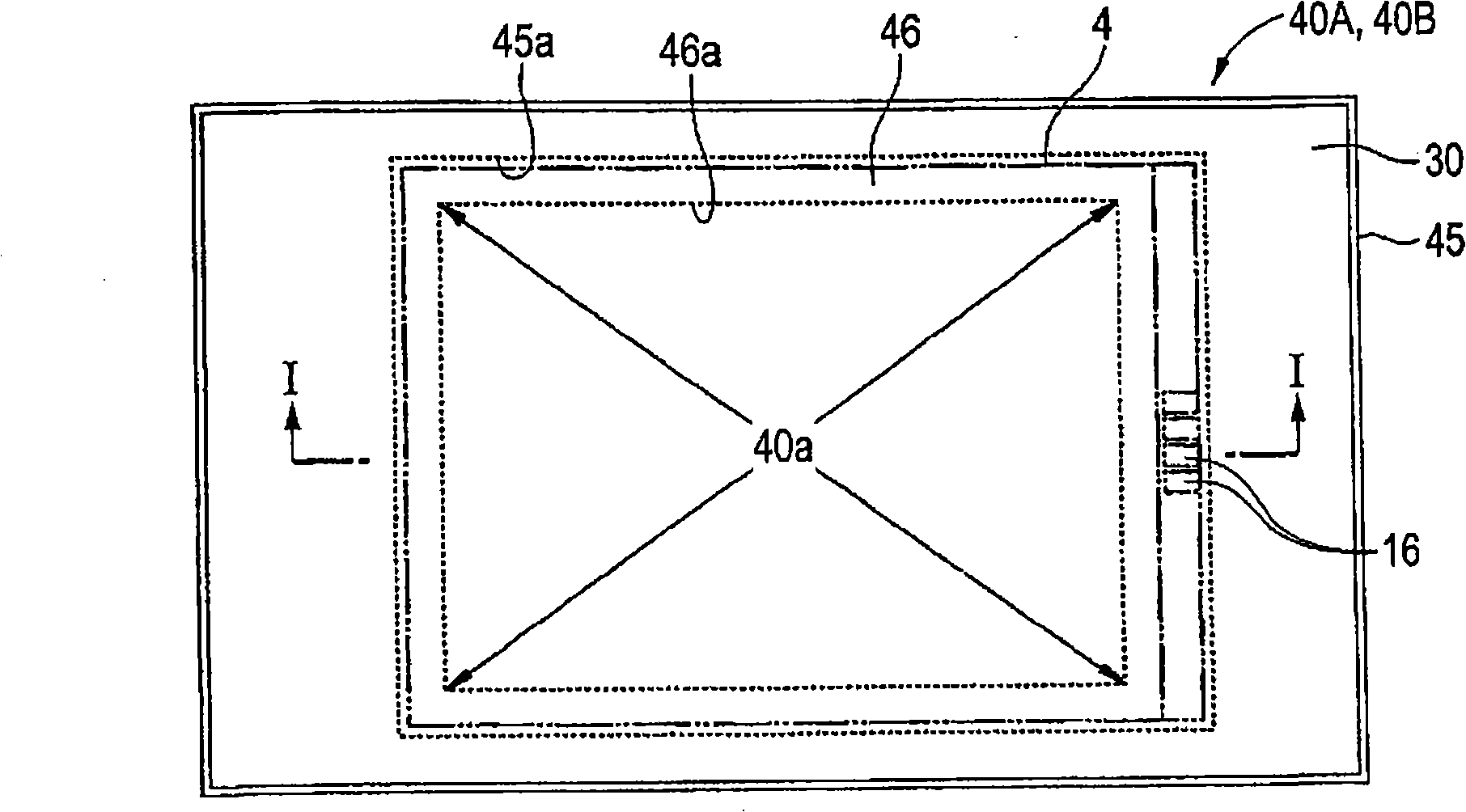
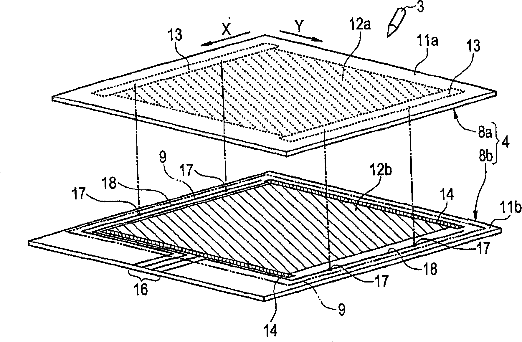
[0080] Fig. 1(a) is a schematic cross-sectional view of an input device 40A in a first configuration example of the first embodiment of the present invention. Fig. 1(b) is also a schematic cross-sectional view of an input device 40B in the second configuration example. figure 2 , is a schematic plan view of the input device 40A shown in FIG. 1 . image 3 , is an exploded perspective view showing the structure of the touch panel 4 .
[0081] (1st configuration example)
[0082] Figure 1 and figure 2 As shown, the input device 40A of this embodiment includes: a cover member 45 having a substantially plate shape in a plan view, and an analog resistive film type touch panel arranged in a storage portion 45 a formed by a rectangular opening formed in the cover member 45 . panel (input panel 4), and the surface 45s on the input operation side of the cover member 45 ( figure 2 The film member (flexible member) 30 bonded to the surface 4 s on the input operation side of the touch ...
no. 2 Embodiment approach
[0148] Next, an electro-optical device as a second embodiment of the present invention will be described with reference to FIGS. 7 to 9 .
[0149] 7( a ) is a schematic cross-sectional view showing a first configuration example of a touch-panel-integrated liquid crystal device as an example of the electro-optical device in the second embodiment. Fig. 8 is a schematic cross-sectional view of a liquid crystal device according to its second configuration example. Fig. 9 is a schematic cross-sectional view of a liquid crystal device according to a third configuration example thereof.
[0150] In addition, although the input device 40B in the second configuration example of the first embodiment or the input device 40D in the fourth configuration example of the first embodiment are described as the input device included in the liquid crystal device in this embodiment, they may be replaced by As the input devices 40B and 40D, input devices 40A, 40C, 40E, and 40F of other configurati...
no. 3 Embodiment approach
[0189] Fig. 10(a) is a schematic cross-sectional view of an input device 40A in the first configuration example of the third embodiment of the present invention. Fig. 10(b) is a schematic cross-sectional view of an input device 40B in its second configuration example. Figure 11 , is a schematic plan view of the input device 40A shown in FIG. 10 . Figure 12 , is an exploded perspective view showing the structure of the touch panel 4 .
[0190] (1st configuration example)
[0191] Figure 10 and Figure 11 As shown, the input device 40A of this embodiment includes: a cover member 45 having a substantially plate shape in a plan view, and an analog resistive film type touch panel arranged in a storage portion 45 a formed by a rectangular opening formed in the cover member 45 . panel (input panel) 4, and the surface 45s on the input operation side of the cover member 45 ( Figure 11 The film member 30 bonded to the surface 4 s on the input operation side of the touch panel 4 ....
PUM
| Property | Measurement | Unit |
|---|---|---|
| thickness | aaaaa | aaaaa |
| thickness | aaaaa | aaaaa |
| width | aaaaa | aaaaa |
Abstract
Description
Claims
Application Information