Display panel and display apparatus including the same
- Summary
- Abstract
- Description
- Claims
- Application Information
AI Technical Summary
Benefits of technology
Problems solved by technology
Method used
Image
Examples
first embodiment
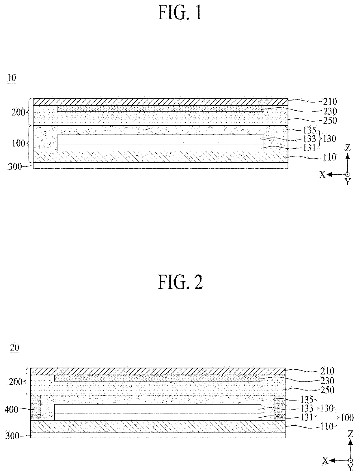
[0047]FIG. 1 illustrates a cross-sectional view of a display panel according to the present disclosure.
[0048]With reference to FIG. 1, the display panel 10 according to the first embodiment of the present disclosure may include a display substrate 100 and a cover substrate 200.
[0049]The display substrate 100 may be defined as a pixel array substrate or a thin film transistor (TFT) array substrate each including a display portion which displays an image (e.g., by emitting light), but is not limited thereto.
[0050]The display substrate 100 according to an embodiment may include a first substrate 110 and a pixel array layer 130.
[0051]The first substrate 110 may be a base substrate of the display substrate 100 and may include a plastic material or a glass material. For example, the first substrate 110 may be formed of a flexible material capable of being curved or bent, and for example, may include opaque or colored polyimide (PI). As another example, the first substrate 110 may be forme...
second embodiment
[0090]FIG. 2 illustrates a cross-sectional view of a display panel 20 according to the present disclosure, and illustrates an embodiment where a sealing member is added to the display panel illustrated in FIG. 1. Hereinafter, therefore, only the sealing member will be described in detail, where like reference numerals refer to like elements as in the other elements of FIG. 1, and repetitive descriptions are omitted or will be briefly given.
[0091]With reference to FIG. 2, in the display panel 20 according to the second embodiment of the present disclosure, a sealing member 400 may be disposed between an edge or a periphery of a display substrate 100 and an edge or a periphery of a cover substrate 200, and may attach the display substrate 100 on the cover substrate 200. Also, the sealing member 400 may surround an outer portion of a pixel array layer 130 disposed on the display substrate 100, and may prevent or block penetration of water or oxygen through side surfaces.
[0092]The seali...
third embodiment
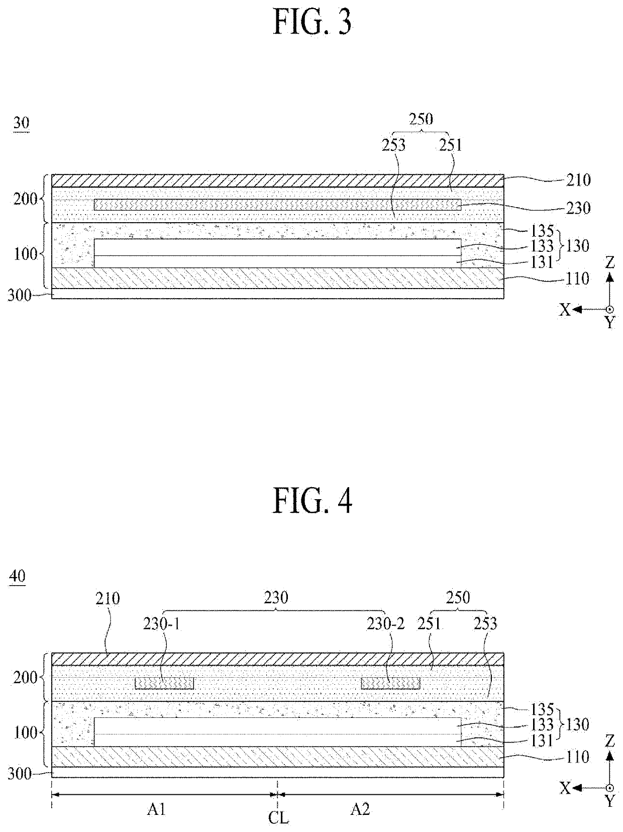
[0097]FIG. 3 illustrates a cross-sectional view of a display panel 30 according to the present disclosure, and illustrates an embodiment implemented by modifying a structure of a cover substrate in the display panel illustrated in FIG. 1. Hereinafter, therefore, only a cover substrate will be described in detail, like reference numerals refer to like elements as in the other elements of FIG. 1, and repetitive descriptions are omitted or will be briefly given.
[0098]With reference to FIG. 3, in the display panel 30 according to the third embodiment of the present disclosure, a cover substrate 200 may include a second substrate 210, a vibration generating module 230, and an adhesive member 250. Except for that the adhesive member 250 is provided to surround an entire surface (or all surfaces) of the vibration generating module 230, the cover substrate 200 may be the same as FIG. 1, and thus, only different elements will be described below.
[0099]The adhesive member 250 according to the ...
PUM
 Abstract
Description
Claims
Application Information


