Stepping arrangement type interference microlithography and device thereof
An arrayed and periodic technology, which is applied in photolithography process exposure devices, microlithography exposure equipment, etc., can solve problems such as application limitations and difficult photoresist material selectivity.
- Summary
- Abstract
- Description
- Claims
- Application Information
AI Technical Summary
Problems solved by technology
Method used
Image

Examples
Embodiment Construction
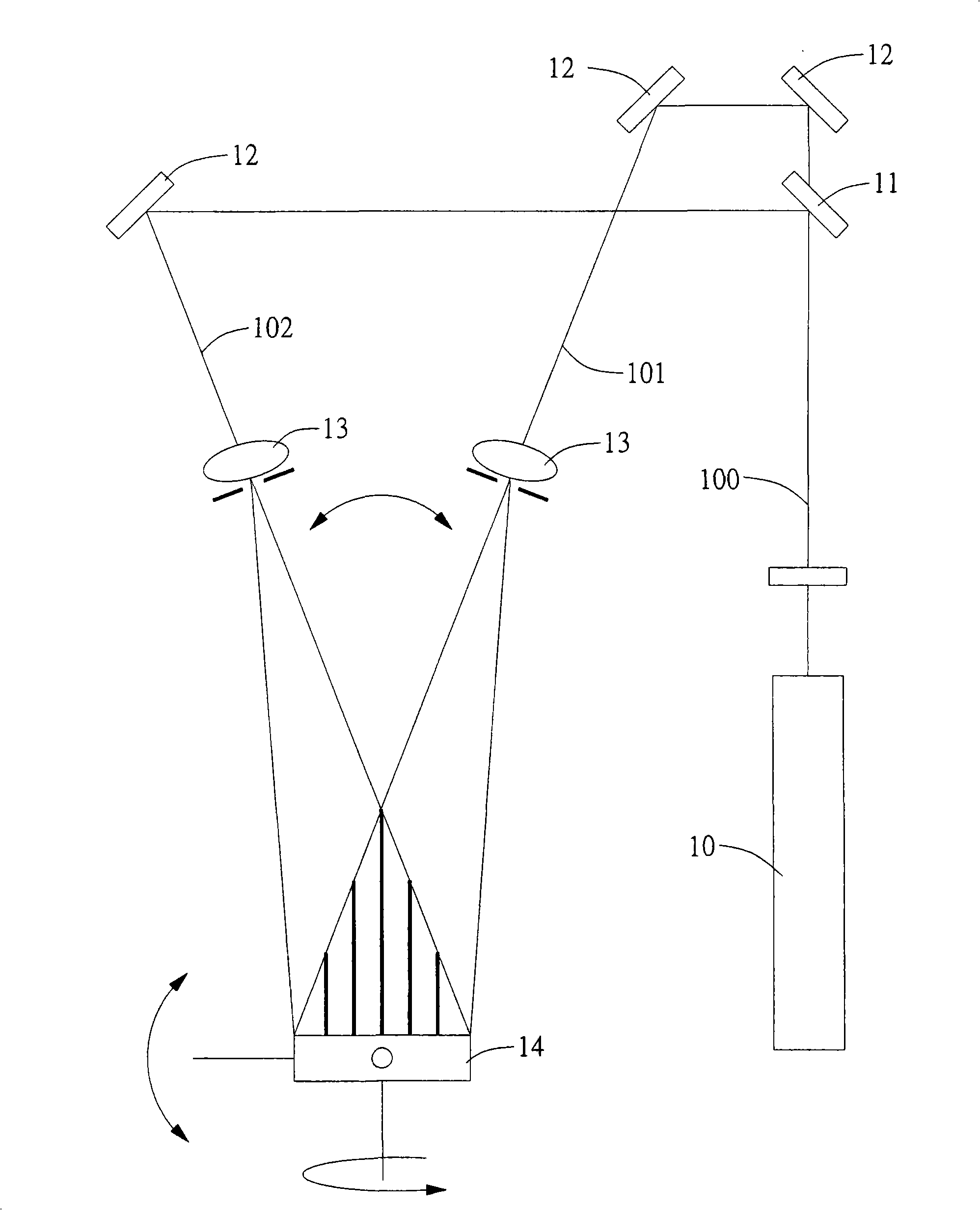
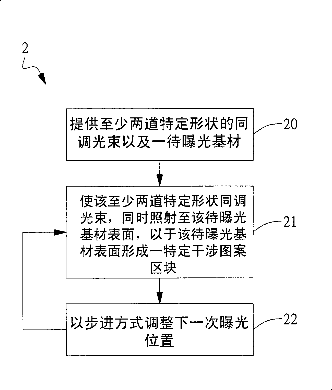
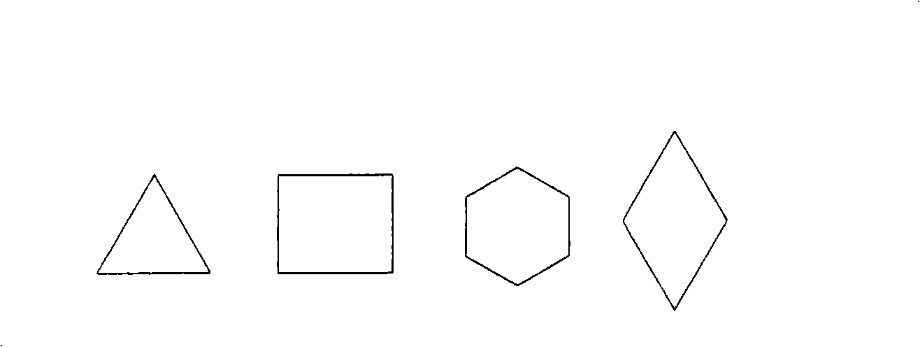
[0062] see figure 2 As shown, this figure is a schematic flow chart of an embodiment of the step-and-array interference lithography method for producing periodic patterns in the present invention. The interference lithography method 2 includes the following steps: first, step 20 is performed, providing at least two coherent light beams of a specific shape and a substrate to be exposed. Please refer to FIG. 3(A), the aforementioned so-called specific shape can be a polygon, such as a triangle, a quadrangle or a hexagon, etc., but not limited thereto. Besides, as shown in FIG. 3(B), the specific shape may also have at least one arc-shaped side. Please refer to FIG. 4(A) and FIG. 4(B), which are schematic diagrams of the present invention to be exposed. In FIG. 3(A), the substrate to be exposed 80 may be a flat substrate; in FIG. 3(B), the substrate to be exposed 81 is a substrate with a curved surface, such as a cylindrical substrate. The materials of the substrates 80 and 8...
PUM
 Abstract
Description
Claims
Application Information
 - R&D Engineer
- R&D Manager
- IP Professional
- Industry Leading Data Capabilities
- Powerful AI technology
- Patent DNA Extraction
Browse by: Latest US Patents, China's latest patents, Technical Efficacy Thesaurus, Application Domain, Technology Topic.
© 2024 PatSnap. All rights reserved.Legal|Privacy policy|Modern Slavery Act Transparency Statement|Sitemap