Chip encapsulating structure
A chip packaging structure and chip packaging technology, applied in the direction of electrical components, electrical solid devices, circuits, etc., can solve the problems of taking a long time, incomplete sealing, unfavorable mass production, etc.
- Summary
- Abstract
- Description
- Claims
- Application Information
AI Technical Summary
Problems solved by technology
Method used
Image


Examples
Embodiment Construction
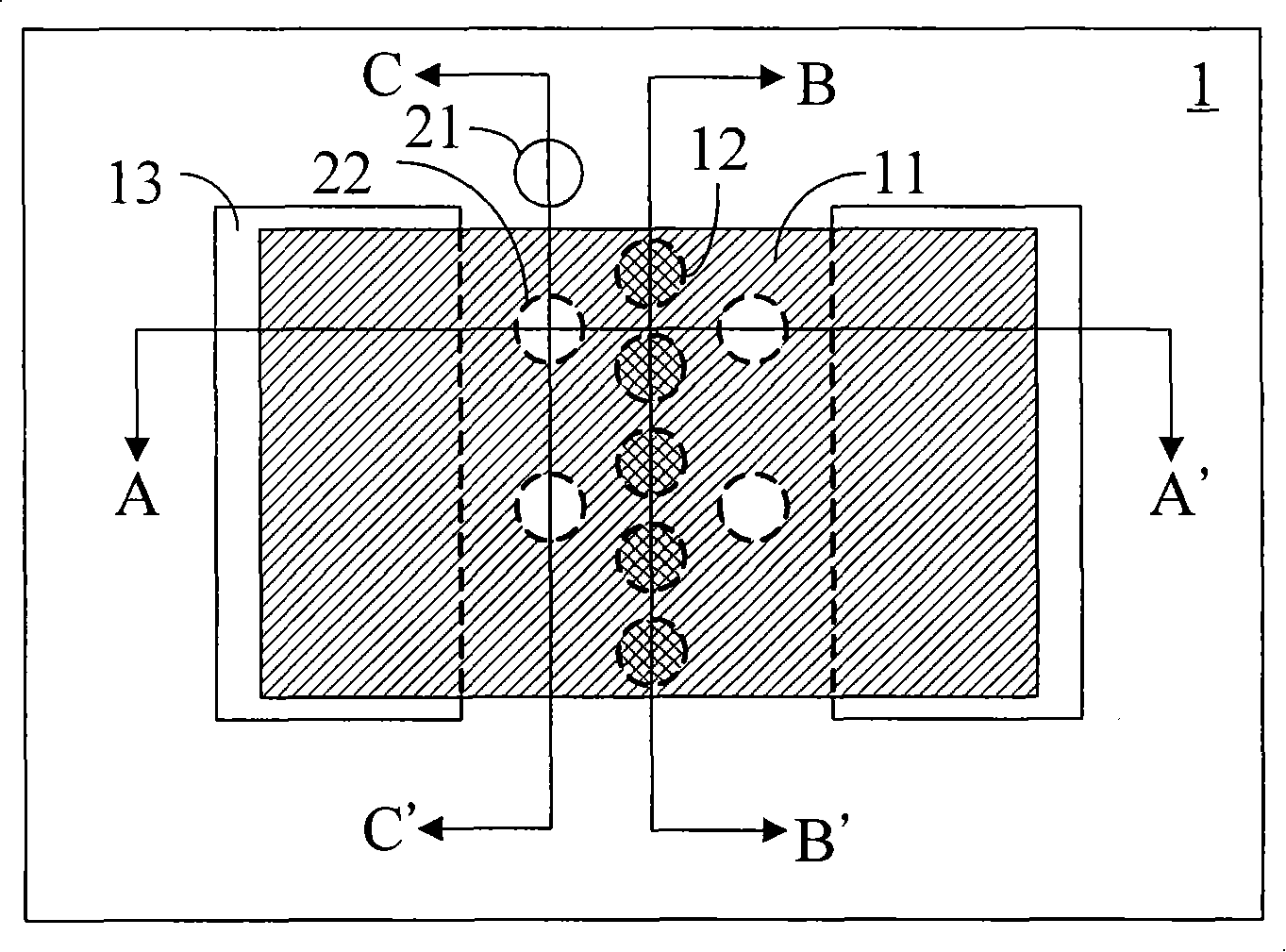
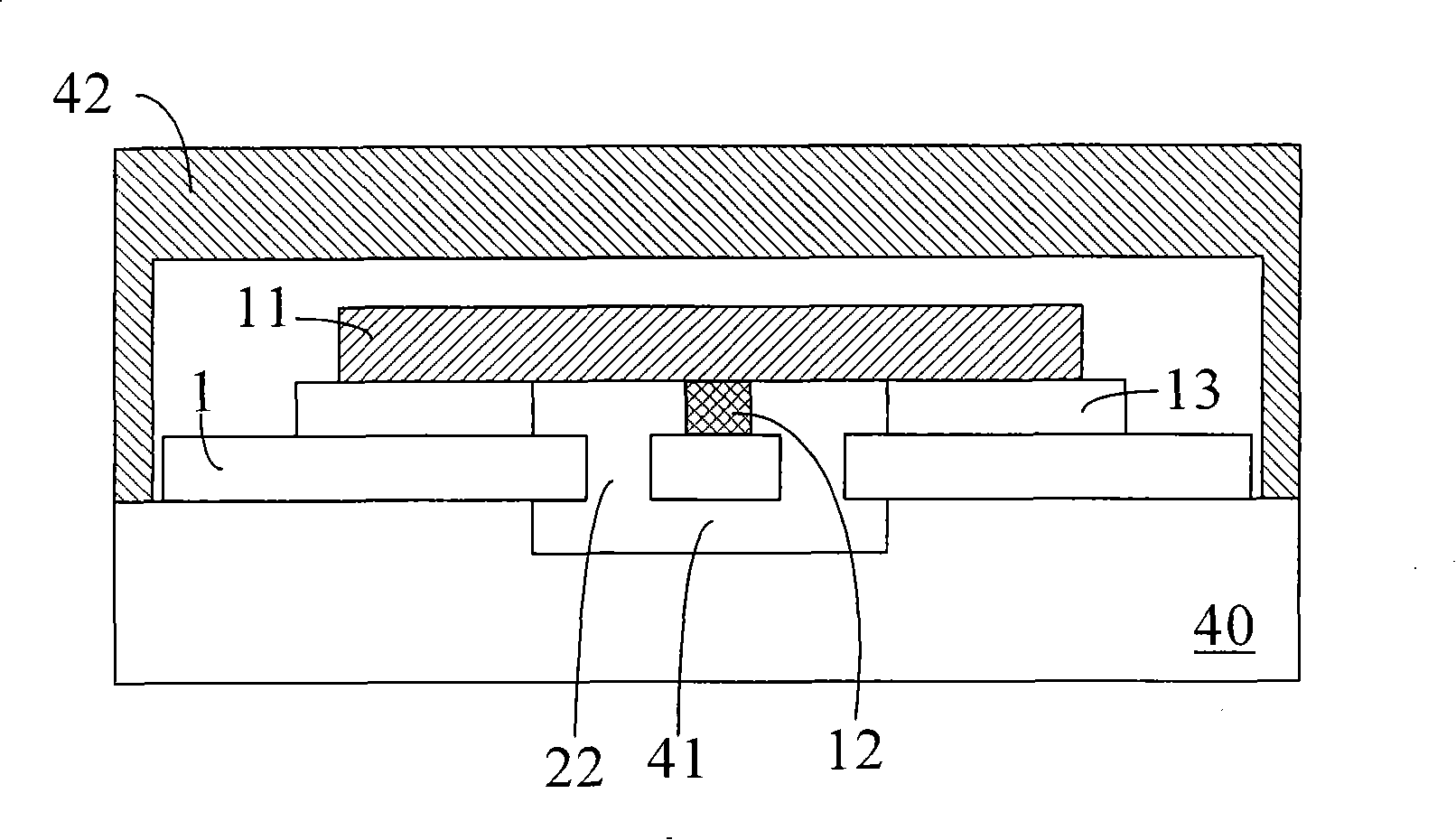
[0026] The content of the present invention will be explained through the following embodiments, which is related to a chip package structure, by providing a plurality of openings on a substrate of the chip package structure, so that at least a part of an injection molding material can pass through at least one of these Holes are opened between a chip and the substrate to form a complete sealant. However, the embodiments of the present invention are not intended to limit the present invention to be implemented in any specific environment, application or special method as described in the embodiments. Therefore, the descriptions about the embodiments are only for the purpose of explaining the present invention rather than limiting the present invention. It should be noted that in the following embodiments and drawings, elements not directly related to the present invention have been omitted and not shown; and for the sake of easy understanding, the dimensional relationship amon...
PUM
 Abstract
Description
Claims
Application Information
 - R&D
- Intellectual Property
- Life Sciences
- Materials
- Tech Scout
- Unparalleled Data Quality
- Higher Quality Content
- 60% Fewer Hallucinations
Browse by: Latest US Patents, China's latest patents, Technical Efficacy Thesaurus, Application Domain, Technology Topic, Popular Technical Reports.
© 2025 PatSnap. All rights reserved.Legal|Privacy policy|Modern Slavery Act Transparency Statement|Sitemap|About US| Contact US: help@patsnap.com