Pixel array and driving method thereof and flat plane display

A flat-panel display and pixel array technology, applied to static indicators, instruments, etc., can solve problems such as bright and dark line defects of even-numbered sub-pixels, display defects of bright and dark lines, and different charging rates between odd-numbered and even-numbered sub-pixels, etc., to improve brightness. Display defects in dark lines, improve the effect of display defects

Active Publication Date: 2011-06-08
AU OPTRONICS CORP
View PDF0 Cites 0 Cited by
  • Summary
  • Abstract
  • Description
  • Claims
  • Application Information

AI Technical Summary

Problems solved by technology

Since the charging time of the HSD pixel array is shorter than that of the traditional architecture, the signal delay effect of the data line and the scan line often affects the gray scale of some sub-pixels
For example, at the end of the data line, the delay of the data line will cause the charging rate of the odd-numbered sub-pixels to be different from that of the even-numbered sub-pixels, resulting in display defects of bright and dark lines
In addition, at the end of the scan line, the delay of the scan line will cause the gate not to be turned off when the polarity is switched, so that even-numbered sub-pixels will have bright and dark line defects due to charging errors

Method used


Image

  • Pixel array and driving method thereof and flat plane display
  • Pixel array and driving method thereof and flat plane display
  • Pixel array and driving method thereof and flat plane display

Examples


no. 1 example

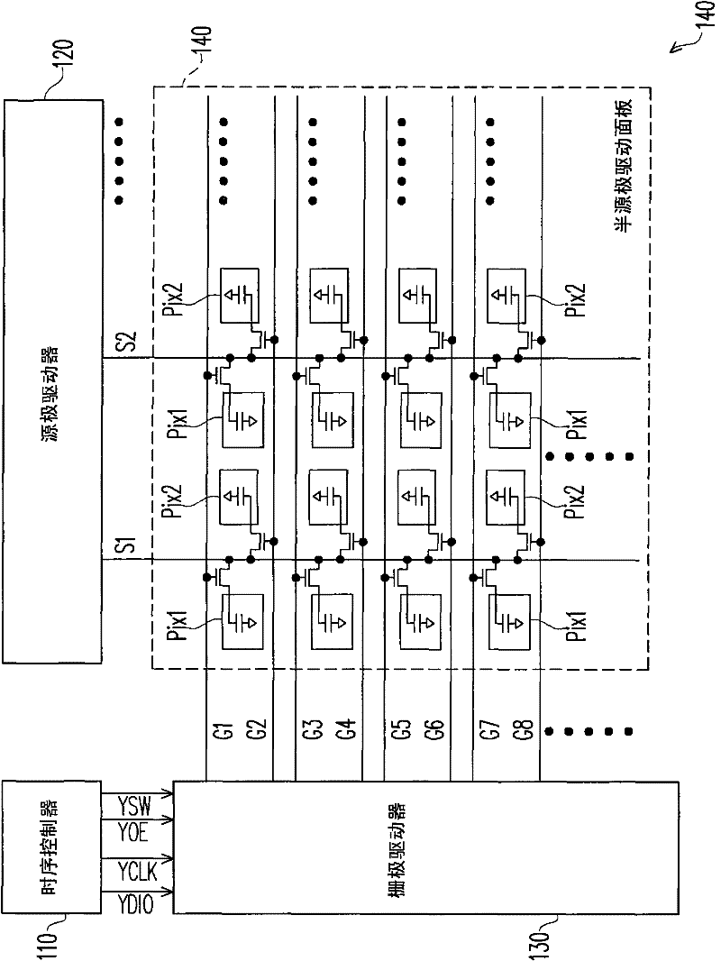
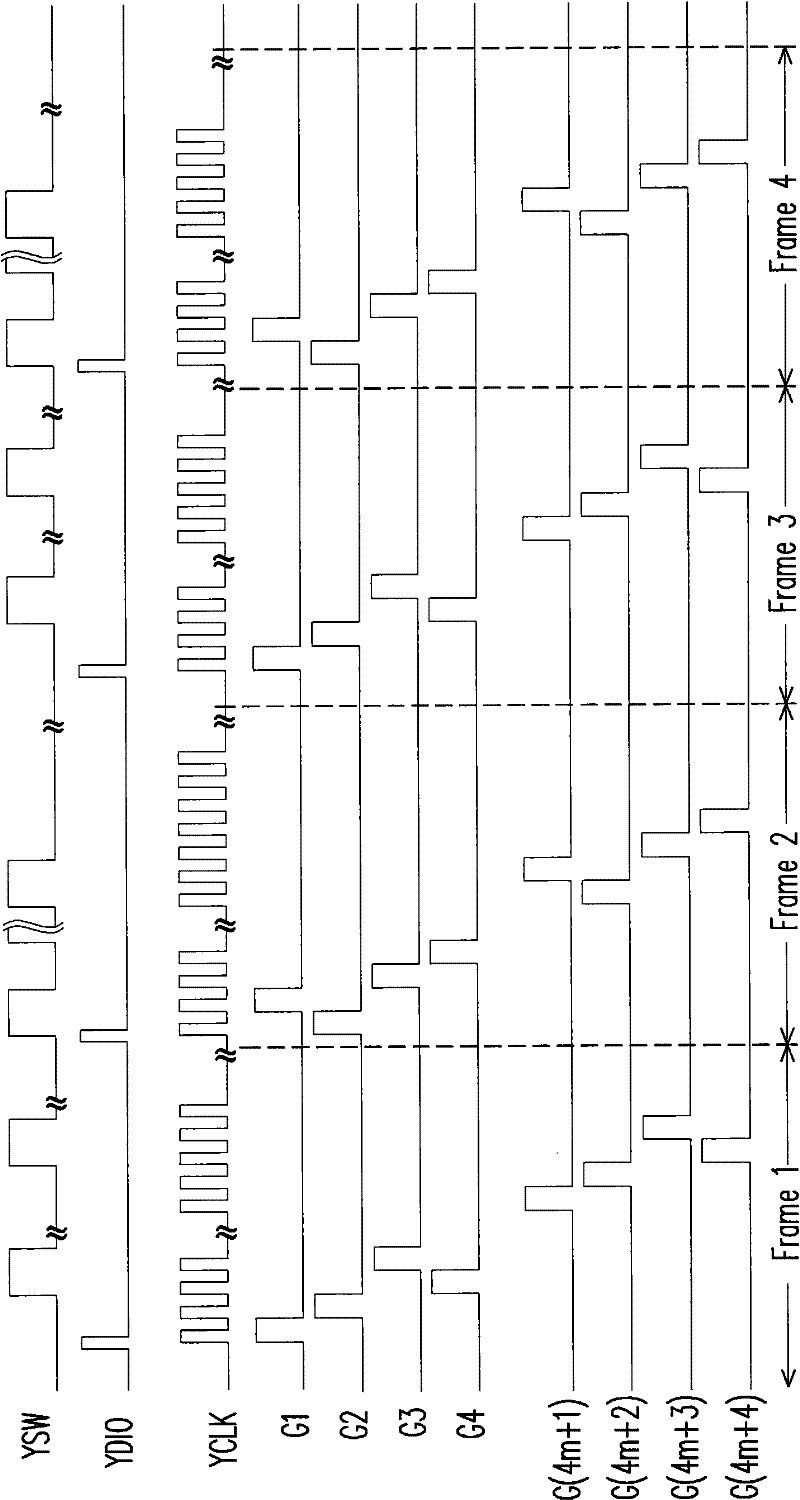
[0045] In this embodiment, the (2n+1)th frame is regarded as the first frame period, and the (2n+2)th frame is regarded as the second frame period, wherein n is an integer. In addition, in this embodiment, the (2m+1)th pixel row of the HSD panel 140 is regarded as the above-mentioned a-th pixel row, and the (2m+2)-th pixel row is regarded as the above-mentioned b-th pixel row, where m is an integer.

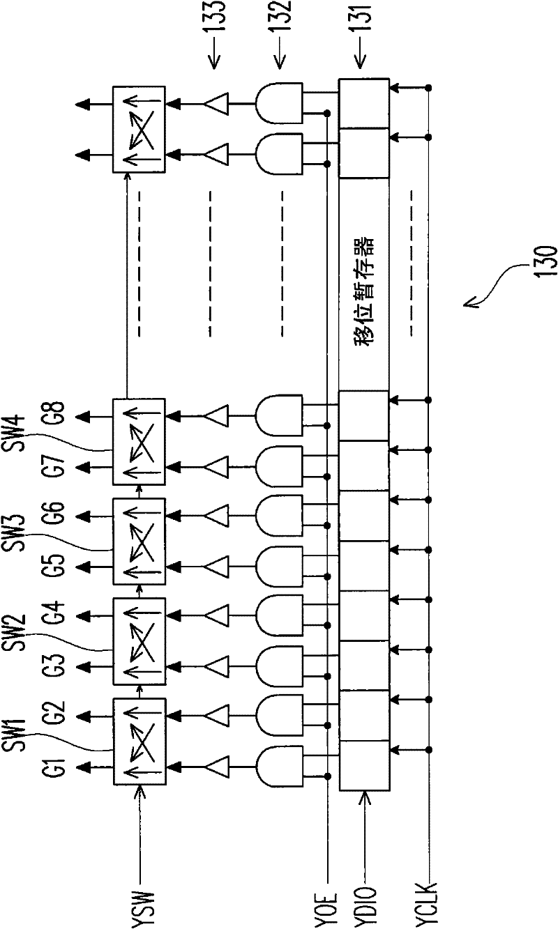
[0046] image 3 In order to illustrate according to this embodiment figure 1 Timing diagram of the medium signal waveform. Please refer to figure 1 and image 3 , at the (2n+1)th frame (eg image 3 In the frame Frame1 or frame Frame3), the gate drive circuit 130 follows the order of "the first scanning line G1, the second scanning line G2, the fourth scanning line G4, the third scanning line G3, ..." , sequentially provide gate driving signals to the HSD panel 140 . That is to say, the gate driving circuit 130 sequentially provides the gate driving signals to Each scan li...

no. 2 example

[0048] Similar to the first embodiment, in this embodiment, the (2n+1)th frame is regarded as the above-mentioned first frame period, and the (2n+2)th frame is regarded as the above-mentioned second frame period. This embodiment is different from the first embodiment in that this embodiment regards the (4m+1)th pixel row of the HSD panel 140 as the above-mentioned a-th pixel row, and uses the (4m+3)th pixel row It is regarded as the b-th pixel row above. During the (2n+1)th frame period, the (4m+1)th pixel row and the (4m+2)th pixel row of the HSD panel 140 are driven in the order of "first scanning line, second scanning line", and The (4m+3)th pixel row and the (4m+4)th pixel row of the HSD panel 140 are driven in the order of "second scan line, first scan line". During the (2n+2)th frame period, the gate driving circuit 130 drives the (4m+1)th pixel row and the (4m+2)th pixel row in the order of "second scanning line, first scanning line" , and the (4m+3)th pixel row and t...

no. 3 example

[0051] Similar to the first embodiment, in this embodiment, the (2n+1)th frame is regarded as the above-mentioned first frame period, and the (2n+2)th frame is regarded as the above-mentioned second frame period. This embodiment is different from the first embodiment in that this embodiment uses 6 pixel rows (that is, 12 scanning lines) as the cycle period. During the first frame period, the gate driving circuit 130 drives the (6m+1)th pixel row and the (6m+2)th pixel row of the HSD panel 140 in the order of "first scanning line, second scanning line" With the (6m+5)th pixel row, the (6m+3)th pixel row and the (6m+4)th pixel row of the HSD panel 140 are driven in the order of "second scan line, first scan line" and the (6m+6)th pixel row. During the second frame period, the gate driving circuit 130 drives the (6m+1) pixel row, the (6m+2) pixel row and the (6m +5) pixel rows, and drive the (6m+3) pixel row, (6m+4) pixel row and (6m+6) pixel row in the order of "the first scan...


PUM


Abstract

The invention relates to a pixel array and a driving method thereof and a flat plane display using the driving method. The pixel array comprises a first scanning line, a second scanning line, a third scanning line and a fourth scanning line. A plurality of pixels are arranged between the first scanning line and the second scanning line. A plurality of pixels are arranged between the third scanning line and the fourth scanning line. During a first frame, a grid driving circuit sequentially provides a driving signal to the first, second, fourth and third scanning lines; and during a second frame, the grid driving circuit sequentially provides a driving signal to the second, first, third and fourth scanning lines. The pixel array and the driving method thereof provided by the invention can avoid the bright and dark line display defect in HSD pixel array driven by the traditional technology.

Description

technical field [0001] The present invention relates to a flat display, in particular to a half source driving panel (half source driving, HSD) pixel array, a driving method thereof, and a flat display. Background technique [0002] With the development of large-sized display panels, among the pixel array structures of current liquid crystal display panels, there is a structure called half source driving (HSD for short). The HSD architecture can halve the number of data lines, so the price of the source driver will be relatively reduced. More specifically, in the pixel array of the HSD architecture, two adjacent sub-pixels share one data line, thereby reducing the number of data lines by half. [0003] However, in the HSD pixel array, in order to maintain the same frame frequency, halving the source driver will cause the charging time of each sub-pixel (about 8~9us) to become less than half of the traditional architecture (18~19us) . Therefore, the charging rate becomes a...

Claims


Application Information

Patent Timeline
Patent Type & Authority Patents(China)
IPC IPC(8): G09G3/20G09G3/36
Inventor 徐兆庆林威呈蔡育均
Owner AU OPTRONICS CORP
Why Eureka
Try Eureka