Method of manufacturing liquid crystal display

a liquid crystal display and manufacturing method technology, applied in the direction of electrical appliances, semiconductor devices, instruments, etc., can solve the problems of unfavorable display, unfavorable display, and spreadability of liquid crystals, and achieve the effect of improving display defects

Active Publication Date: 2015-01-22
SAMSUNG DISPLAY CO LTD
View PDF5 Cites 0 Cited by
  • Summary
  • Abstract
  • Description
  • Claims
  • Application Information

AI Technical Summary

Benefits of technology

[0005]Exemplary embodiments of the present invention provide a method of manufacturing a liquid crystal display which can improve display defects such as, for example, mura that may occur due to non-uniformity of a liquid crystal layer caused by steps formed within the liquid crystal display.

Problems solved by technology

During the manufacturing of a liquid crystal display, an unnecessary step may be generated between a light blocking area in which a light blocking member is formed and a transmission area in which the light blocking member is not formed.
Due to the step between the light blocking area and the transmission area, spreadability of the liquid crystals of the liquid crystal layer may deteriorate during a process of injecting the liquid crystal layer between the two display panels, and as a result, mura due to non-uniformity of the liquid crystal layer may be generated.

Method used


Image

  • Method of manufacturing liquid crystal display
  • Method of manufacturing liquid crystal display
  • Method of manufacturing liquid crystal display

Examples


Embodiment Construction

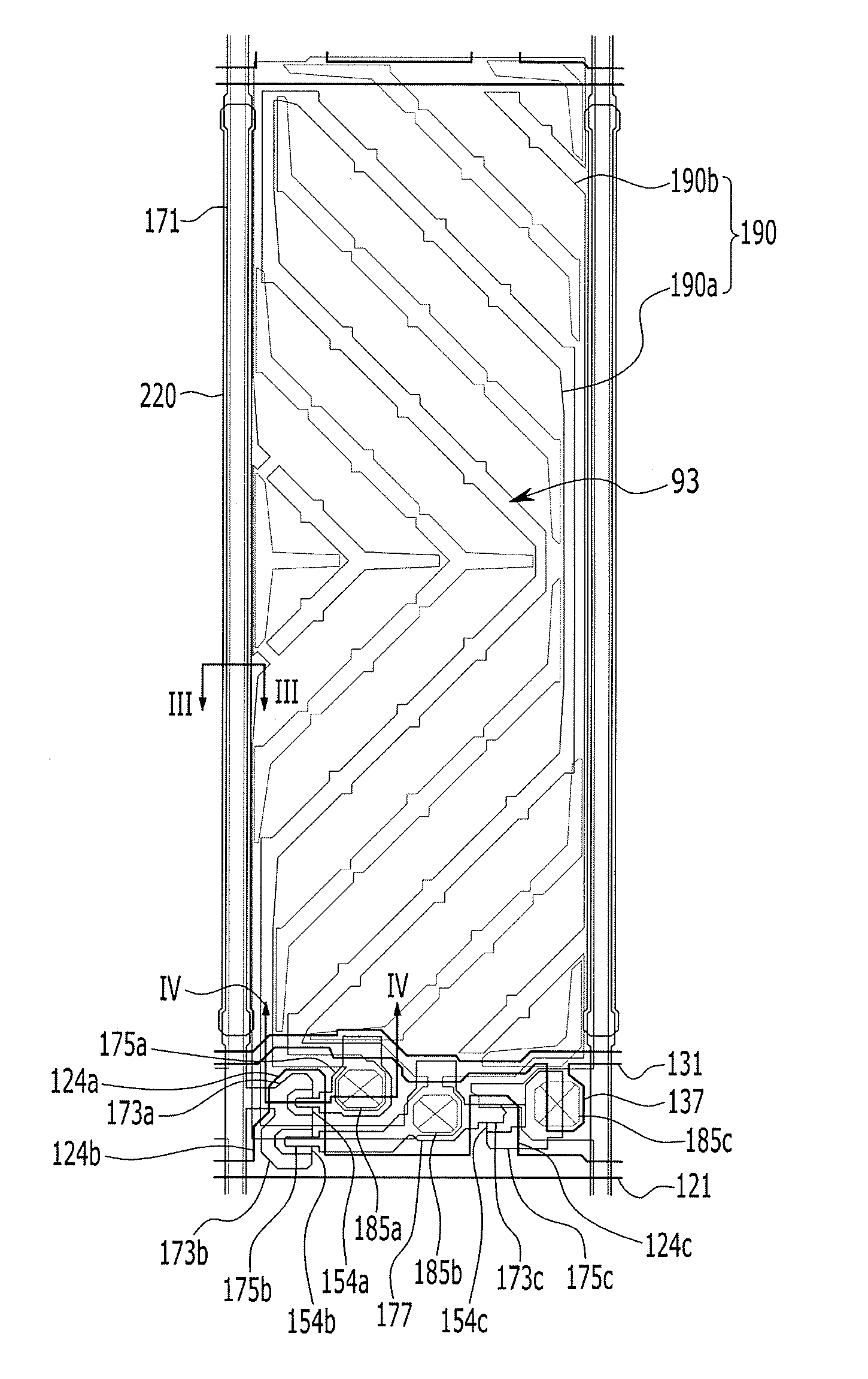
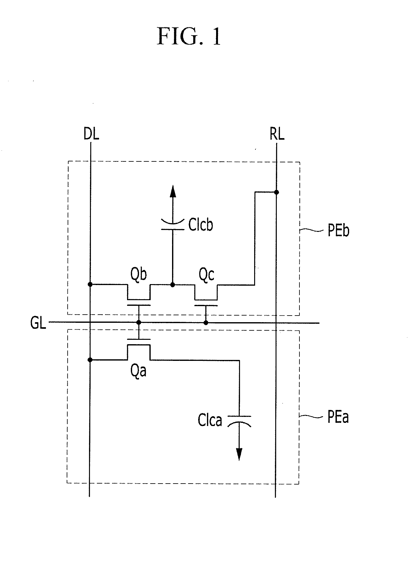
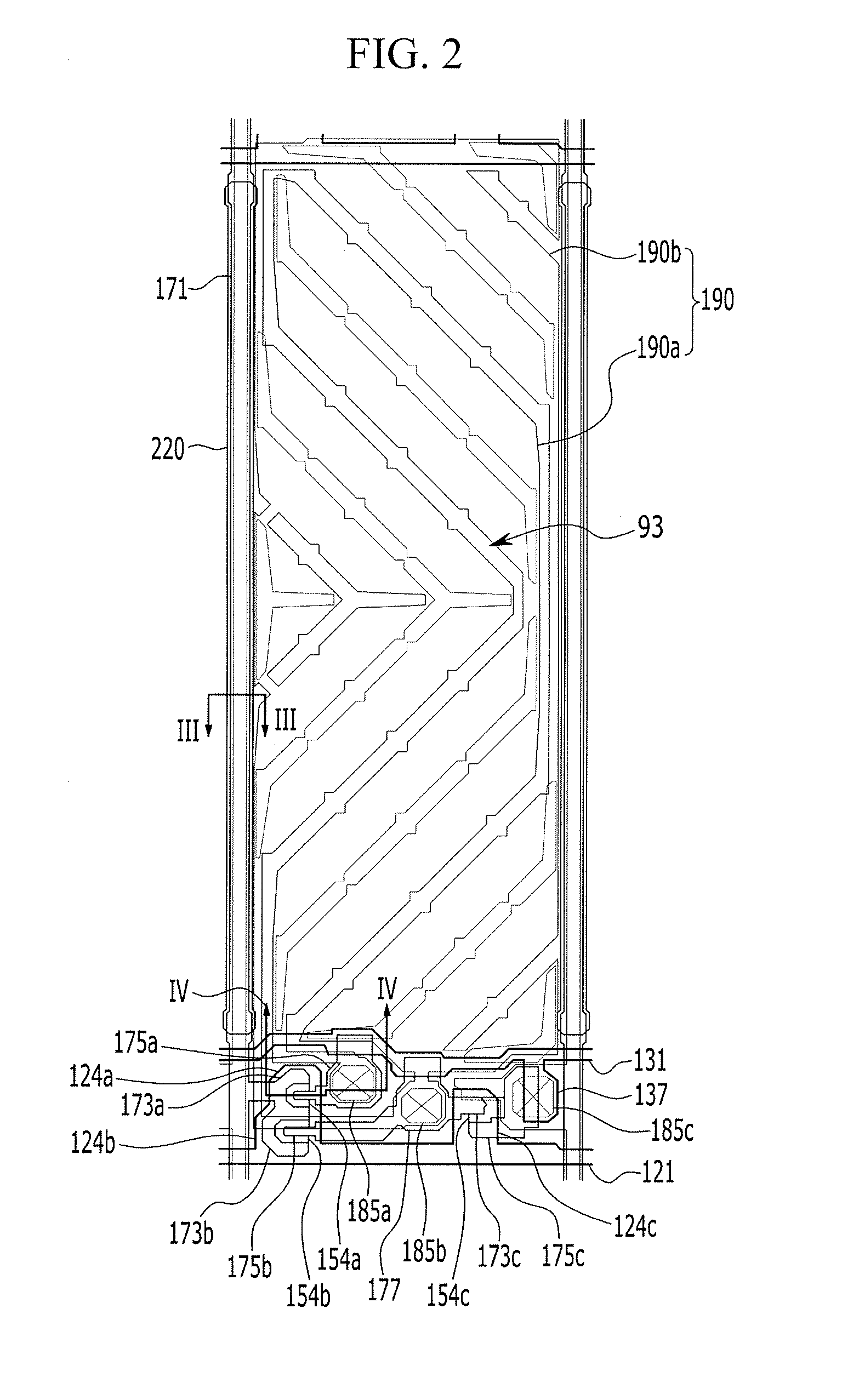
[0028]Exemplary embodiments of the present invention will be described more fully hereinafter with reference to the accompanying drawings. Like reference numerals may refer to like elements throughout the accompanying drawings.

[0029]In the drawings, the thickness of layers, films, panels, regions, etc., may be exaggerated for clarity. It will be understood that when an element or layer is referred to as being “on” another element or layer, it can be directly on the other element or layer or intervening elements or layers may also be present. Spatially relative terms, such as “beneath”, “below”, “lower”, “under”, “above”, “upper” and the like, may be used herein for ease of description to describe one element or feature's relationship to another element(s) or feature(s) as illustrated in the figures. It will be understood that the spatially relative terms are intended to encompass different orientations of the device in use or operation in addition to the orientation depicted in the ...


PUM

PropertyMeasurementUnit
angleaaaaaaaaaa
areaaaaaaaaaaa
insulatingaaaaaaaaaa

Abstract

A method of manufacturing a liquid crystal display includes disposing a gate electrode and a light blocking member on a substrate, disposing a source electrode and a drain electrode on the gate electrode to form a thin film transistor, disposing a data line on the light blocking member, disposing an organic layer on the thin film transistor and the data line, exposing a first convex part of the organic layer to light in a first area corresponding to the thin film transistor during an exposure process, and exposing a second convex part of the organic layer to the light in a second area corresponding to the data line during the exposure process using a mask. The mask includes a first transflective part aligned with the first area and a second transflective part aligned with the second area during the exposure process.

Description

CROSS-REFERENCE TO RELATED APPLICATIONS[0001]This application claims priority under 35 U.S.C. §119 to Korean Patent Application No. 10-2013-0084948 filed on Jul. 18, 2013, the disclosure of which is incorporated by reference herein in its entirety.TECHNICAL FIELD[0002]Exemplary embodiments of the present invention relate to a method of manufacturing a liquid crystal display, and more particularly, to a method of manufacturing a liquid crystal display in which a step between a light blocking area and a transmission area is reduced or eliminated.Discussion of the Related Art[0003]A liquid crystal display includes two display panels on which electric field generating electrodes such as a pixel electrode and a common electrode are formed, and a liquid crystal layer disposed between the two display panels. The liquid crystal display displays an image by applying a voltage to the electric field generating electrodes to generate an electric field in the liquid crystal layer, changing the o...

Claims


Application Information

Patent Timeline
Patent Type & Authority Applications(United States)
IPC IPC(8): H01L27/12G02F1/1333
CPCH01L27/1296G02F1/1333G02F1/136209G02F2001/13625H01L27/1288G02F1/13625G02F1/1343G02F1/136
Inventor SHIM, SEUNG BOKIM, JUN GIJUNG, YANG-HOJU, JIN HOPARK, JUN HONG
Owner SAMSUNG DISPLAY CO LTD
Why Eureka
Try Eureka