
Pixel array

A pixel array and pixel column technology, applied in the field of pixel arrays, can solve the problems of alternating bright and dark lines, affecting the display quality of flat-panel displays, etc., and achieve the effect of improving display quality and improving display defects.

Inactive Publication Date: 2011-06-15
AU OPTRONICS CORP
View PDF0 Cites 0 Cited by
  • Summary
  • Abstract
  • Description
  • Claims
  • Application Information

AI Technical Summary

Problems solved by technology

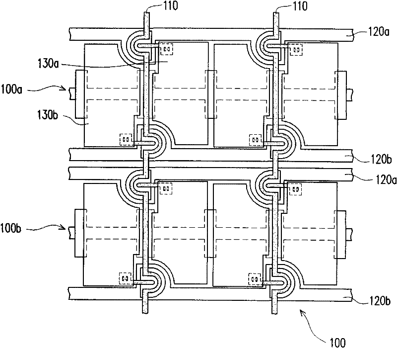
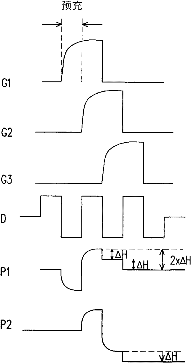
In this way, when the first sub-pixel 130a and the second sub-pixel 130b are displaying, there will be a display defect of alternating bright and dark lines, which will further affect the display quality of the flat-panel display.

Method used


Image

  • Pixel array
  • Pixel array
  • Pixel array

Examples


Embodiment Construction

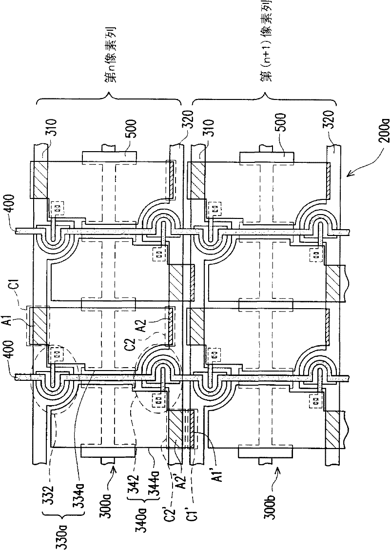
[0056] Figure 2A It is a schematic diagram of a pixel array according to the first embodiment of the present invention. Please refer to Figure 2A , the pixel array 200 a includes a plurality of pixel columns 300 a, 300 b and a plurality of data lines 400 . In detail, the pixel row 300 a (or the pixel row 300 b ) includes a first scan line 310 , a second scan line 320 , a plurality of first sub-pixels 330 a and a plurality of second sub-pixels 340 a. Wherein, the first scan lines 310 and the second scan lines 320 in the pixel column 330 a are arranged alternately with the first scan lines 310 and the second scan lines 320 in the pixel column 330 b. The first sub-pixel 330a and the second sub-pixel 340a are alternately arranged between the first scanning line 310 and the second scanning line 320, wherein the first sub-pixel 330a is electrically connected to the first scanning line 310, and the second sub-pixel 340a It is electrically connected with the second scan line 320 ...


PUM


Abstract

The invention provides a pixel array comprising a plurality of pixel rows and a plurality of data wires, wherein each pixel row comprises a first scanning line, a second scanning line, a plurality of first sub-pixels and a plurality of second sub-pixels; the first sub-pixels and the second sub-pixels are alternately distributed between the first scanning line and the second scanning line; the data wires, the first scanning line and the second scanning line are arranged in a staggered manner; and part of the first sub-pixels and part of the second sub-pixels electrically connected with the same data wire are located on two opposite sides of the data wire respectively. In the nth pixel row, the sum of C1 and C2 is substantially equal to that of C1' and C2', wherein C1 represents the coupling capacitance of each first sub-pixel and the first scanning line, and C2 represents the coupling capacitance of each second sub-pixel and the second scanning line; and C1' represents the coupling capacitance of each second sub-pixel and the first scanning line in the (n+1)th pixel row, and C2' represents the coupling capacitance of each second sub-pixel and the second scanning line.

Description

technical field [0001] The present invention relates to a pixel array, and in particular to a pixel array with Half Source Driver (HSD) architecture. Background technique [0002] Generally speaking, a flat panel display is mainly composed of a display panel and a plurality of driver ICs, wherein the display panel has a pixel array, and the pixels of the pixel array are driven by corresponding scan lines and corresponding data lines. In order to make flat-panel displays more popular, the industry is in full swing to reduce costs. In recent years, a data-driven chip half-source driver (Half Source Driver, HSD) architecture design has been proposed, which mainly uses the layout of the pixel array to reduce the cost. Data drives chip usage. Specifically, in the pixel array of the HSD architecture, two adjacent sub-pixels (sub-pixel) share the same data line, so the total number of data lines can be halved, but the total number of scanning lines is doubled. . Since the HSD ar...

Claims


Application Information

Patent Timeline
Patent Type & Authority Patents(China)
IPC IPC(8): G02F1/1362
Inventor 江博仁刘晋炜
Owner AU OPTRONICS CORP
Learn More