
Display cell

A display unit and substrate technology, applied in nonlinear optics, instruments, optics, etc., can solve problems such as inability to separate the useless substrate W, weak strength, broken CF substrate 130, etc., and achieve the effect of suppressing poor segmentation

Active Publication Date: 2010-03-24
SHARP KK
View PDF2 Cites 13 Cited by
  • Summary
  • Abstract
  • Description
  • Claims
  • Application Information

AI Technical Summary

Problems solved by technology

like Figure 11 As shown, in this liquid crystal cell, the sealing material 125 on the side of the terminal region T is extended to the line P to be divided.
In this way, when the CF substrate 130 is thin, since the strength of the substrate itself is weak, even if the CF substrate 130 is forcibly torn off, not only the useless substrate W cannot be separated at the normal position (planned dividing line P), but the CF substrate is often broken. 130 broken with useless substrate W

Method used


Image

  • Display cell
  • Display cell
  • Display cell

Examples


Embodiment approach 1

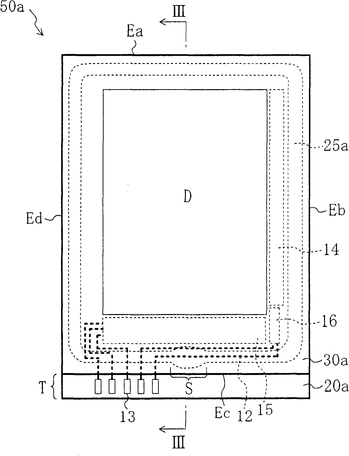
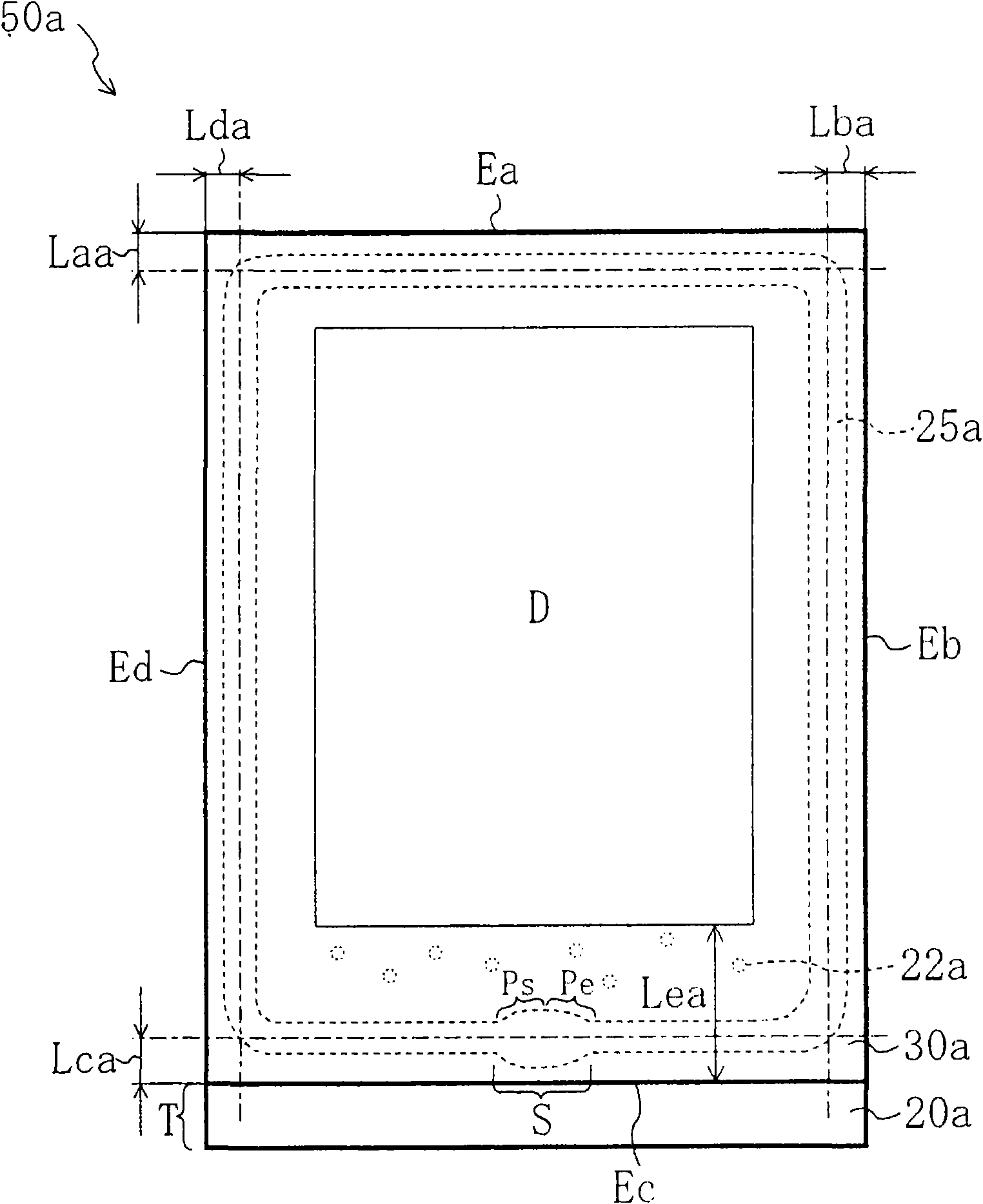
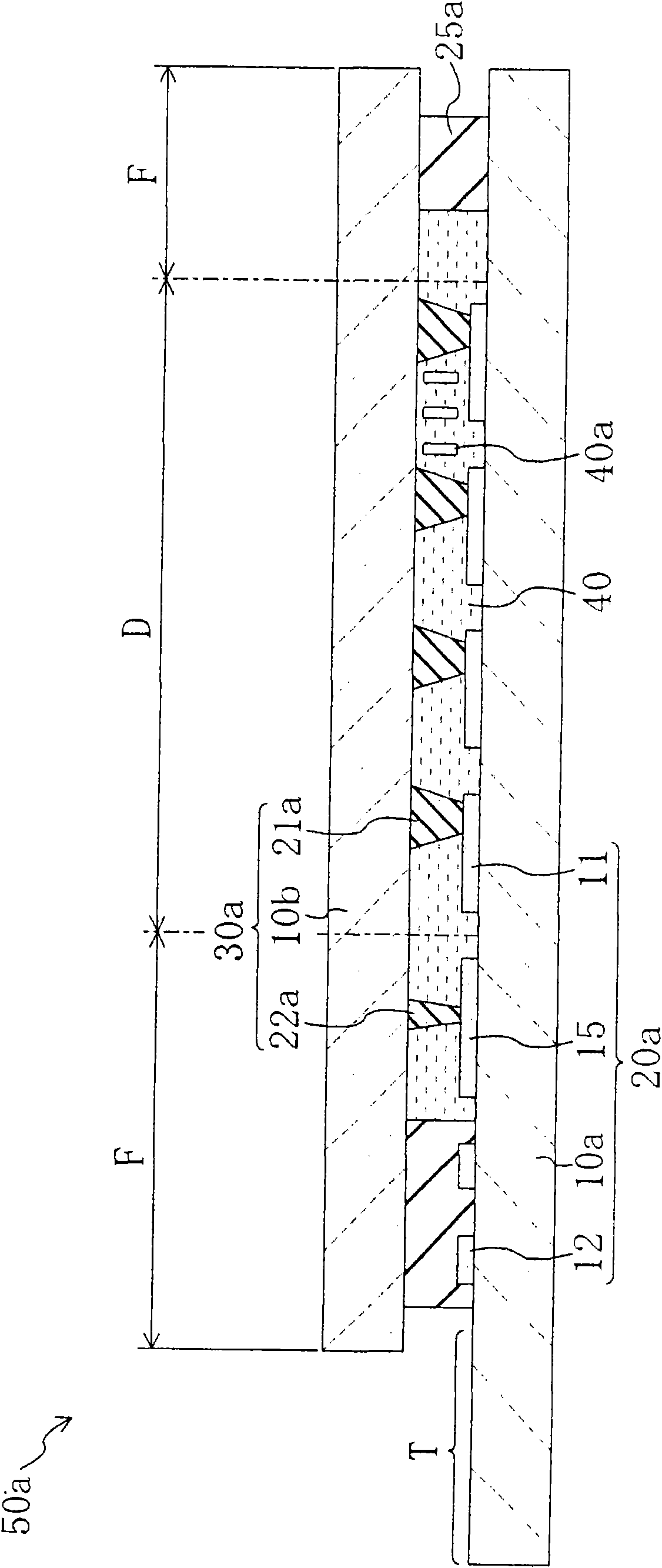
[0069] Figure 1 ~ Figure 3 Embodiment 1 of the display unit (liquid crystal unit) of the present invention is shown.

[0070] Specifically, figure 1 is a plan view of the liquid crystal cell 50a of this embodiment, figure 2 is a plan view for explaining the structure of the sealing material 25a of the liquid crystal cell 50a, and image 3 is along figure 1 A cross-sectional view of the liquid crystal cell 50a on line III-III.

[0071] Such as Figure 1 ~ Figure 3 As shown, the liquid crystal unit 50a includes: a TFT substrate 20a as a first substrate, a CF substrate 30a as a second substrate disposed opposite to the TFT substrate 20a, a liquid crystal layer 40 between the TFT substrate 20a and the CF substrate 30a, and a TFT The substrate 20 a and the CF substrate 30 a are bonded to each other, and a frame-shaped sealing material 25 a of the liquid crystal layer 40 is sealed between the TFT substrate 20 a and the CF substrate 30 a.

[0072] Additionally, if Figure ...

Embodiment approach 2

[0114] Figure 4 ~ Figure 6 Embodiment 2 of the display unit (liquid crystal unit) of the present invention is shown. In addition, in each of the following embodiments, with Figure 1 ~ Figure 3 For the same parts, the same symbols are used, and detailed description thereof will be omitted.

[0115] In Embodiment 1 described above, the structure in which the gate driver circuit 14 and the source driver circuit 15 are monolithically formed was exemplified, but the present invention is not limited to this structure.

[0116] Specifically, Figure 4 is a plan view of the liquid crystal cell 50b of this embodiment, Figure 5 is a plan view for explaining the structure of the sealing material 25a of the liquid crystal cell 50b, and Figure 6 is along Figure 4 A cross-sectional view of the liquid crystal cell 50b on line VI-VI.

[0117] Such as Figure 4 ~ Figure 6 As shown, the liquid crystal unit 50b has: a first substrate, namely a TFT substrate 20b; a second substrate di...

Embodiment approach 3

[0139] Figure 7 Embodiment 3 of the display unit (liquid crystal unit) of the present invention is shown. Specifically, Figure 7 It is a plan view which shows the liquid crystal cell 50c of this embodiment.

[0140] In each of the above-mentioned embodiments, the sealing material 25a on one side having the sealing joint S is uniformly far from the end of the CF substrate from one end to the other end of the side, but in this embodiment, only the sealing material 25a having the sealing joint S A part of one side of the sealing material 25b is bent toward the display region D side, and a sealing joint S is formed at this part.

[0141] According to the liquid crystal cell 50c of this embodiment, since the sealing joint part S of the sealing material 25b is away from the edge part of the CF board|substrate 30a similarly to each of the above-mentioned embodiment, the division defect by the sealing joint part S can be suppressed.


PUM


Abstract

A liquid crystal cell (50a) is provided with a TFT substrate (20a); terminal region (T) specified along one side of the TFT substrate (20a); a CF substrate (30a) arranged to face the TFT substrate (20a) so that the terminal region (T) is exposed; a frame-like seal material (25a) having a widely formed seal connecting section (S); a display region (D) specified inside the seal material (25a); and four frame side region specified by the periphery of the display region (D) with the seal material (25a) arranged thereon. The seal material (25a) is arranged by being more spaced apart from an end section of the CF substrate (30a) compared with other three frame side regions and has a seal connecting section (S) in the widest one frame side region among the four frame side regions. Since the sealconnecting section (S) is spaced apart from the end section of the CF substrate (30a), divided failure of the liquid crystal cell (50a) can be suppressed. The liquid crystal cell (50a) can be used, for instance, for a cellular phone.

Description

technical field [0001] The present invention relates to a display unit manufactured by bonding a pair of substrates together with a sealing material, and particularly relates to a liquid crystal cell manufactured by a drop injection method. Background technique [0002] A typical liquid crystal cell has a structure in which a first substrate and a second substrate having different sizes are bonded together with a frame-shaped sealing material. In addition, electrodes for applying a voltage to the liquid crystal layer sandwiched between the first substrate and the second substrate are arranged facing each other on the respective surfaces of the first substrate and the second substrate. [0003] Figure 8 is a plan view of a conventional liquid crystal cell 150a in which a monolithic circuit is formed in a substrate, Figure 9 It is a plan view for explaining the structure of the sealing material 125a of the liquid crystal cell 150a. [0004] Such as Figure 8 and Figure 9...

Claims


Application Information

Patent Timeline
Patent Type & Authority Applications(China)
IPC IPC(8): G02F1/1339G02F1/1345
CPCG02F2001/13415G02F1/1339G02F1/1341G02F1/13452G02F1/13415
Inventor 藤川阳介
Owner SHARP KK
Learn More