Photoelectric device with variable resistor structure

A resistance structure and photoelectric device technology, which is applied in the direction of circuits, electrical components, and electrical solid-state devices, can solve the problems of unable to improve production efficiency, labor and time consumption, etc.

Inactive Publication Date: 2010-12-22
EPISTAR CORP
View PDF0 Cites 0 Cited by
  • Summary
  • Abstract
  • Description
  • Claims
  • Application Information

AI Technical Summary

Problems solved by technology

However, it is labor-intensive and time-consuming to carry out point measurement and laser trimming at the same time, so that the production efficiency cannot be improved

Method used


Image

  • Photoelectric device with variable resistor structure
  • Photoelectric device with variable resistor structure
  • Photoelectric device with variable resistor structure

Examples


Embodiment Construction

[0034] Embodiments of the present invention will be described in detail and drawn in the drawings, and the same or similar parts will appear in the drawings and descriptions with the same symbols.

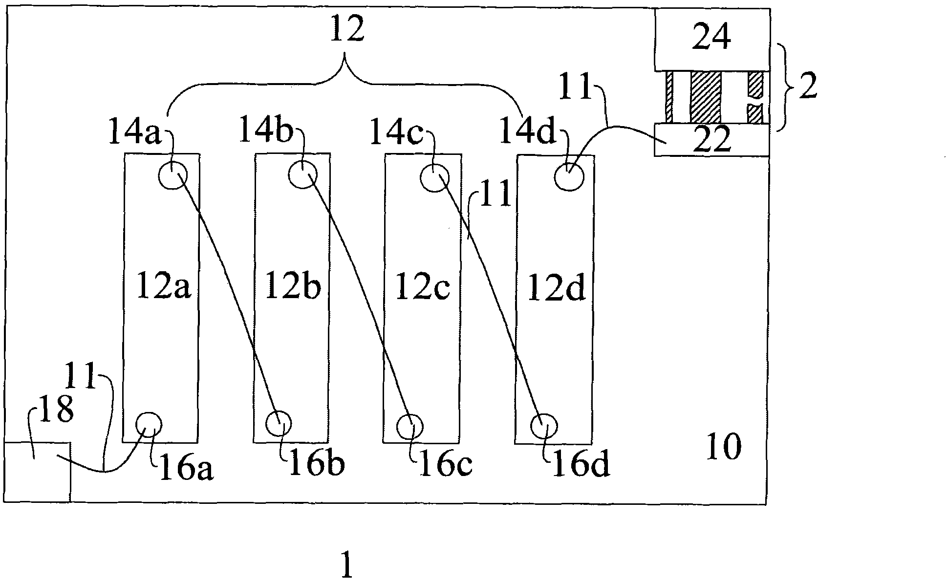
[0035] Such as figure 1 As shown, the first embodiment of the photoelectric device 1 having a variable resistance structure includes a substrate 10; a photoelectric element array 12 is formed on the substrate 10, wherein the photoelectric element array 12 includes a first photoelectric element 12a, a second photoelectric element 12b, The third photoelectric element 12c and the fourth photoelectric element 12d. Here, the photoelectric elements of the photoelectric element array 12 are connected in series as an example. The first electrode 14a of the first photoelectric element 12a and the first electrode of the second photoelectric element 12b 14b and the first electrode 14c of the third photoelectric element 12c are respectively connected to the second electrode 16b of the second ...


PUM


Abstract

A photoelectric device with a variable resistor structure comprises a substrate, wherein a photoelectric element array is arranged on the substrate; the photoelectric element array is electrically connected with the variable resistor structure via a conductor structure; and at least a resistor in the variable resistor structure is disconnected.

Description

technical field [0001] The invention relates to a photoelectric device, in particular to a photoelectric device with a variable resistance structure. Background technique [0002] There are many types of optoelectronic elements, such as light-emitting diodes (Light-emitting Diode; LED), solar cells (Solar Cell) or photodiodes (Photo diode). Taking the LED array as an example, the LED array has many applications, such as lighting devices or display devices, and the required operating voltage and current are different according to different applications. Therefore, the LED array will be electrically connected with some resistors to adjust the voltage or current. [0003] Before electrically connecting the resistor to the LED array, the resistance value of the resistor is generally adjusted by means of laser trimming. Figure 7 It is a schematic diagram of the path of the laser on the resistance, such as Figure 7 As shown, in order to accurately adjust the resistance value of...

Claims


Application Information

Patent Timeline
Patent Type & Authority Applications(China)
IPC IPC(8): H01L25/16H01L33/00
Inventor 许嘉良
Owner EPISTAR CORP
Why Eureka
Try Eureka