
Green field effect transistor and manufacturing method thereof
A field-effect transistor and manufacturing method technology, which is applied in semiconductor/solid-state device manufacturing, semiconductor devices, electrical components, etc., can solve the problem of unreported semiconductor manufacturing process, avoid secondary effects, small sub-threshold swing, and switch Feature Sensitive Effects
- Summary
- Abstract
- Description
- Claims
- Application Information
AI Technical Summary
Problems solved by technology
Method used
Image

Examples
Embodiment Construction
[0045] It is known from the prior art that green transistors have lower energy consumption and stable device characteristics in a small size, which meets the low energy consumption requirements of VDD scaling down. On this basis, the present invention provides a new green field effect transistor.
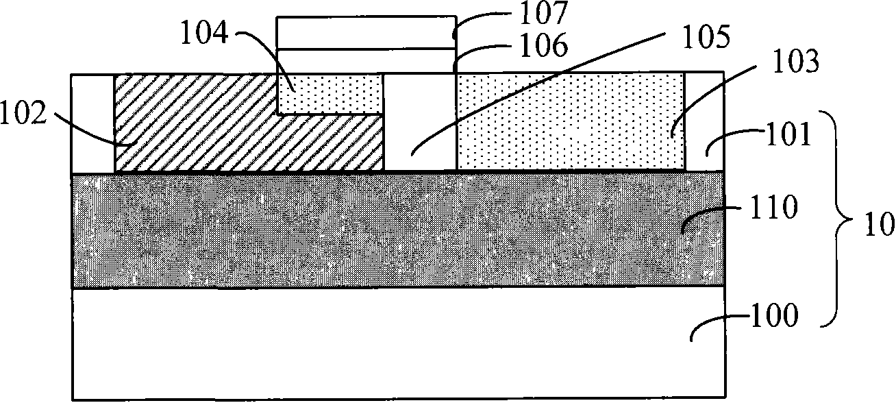
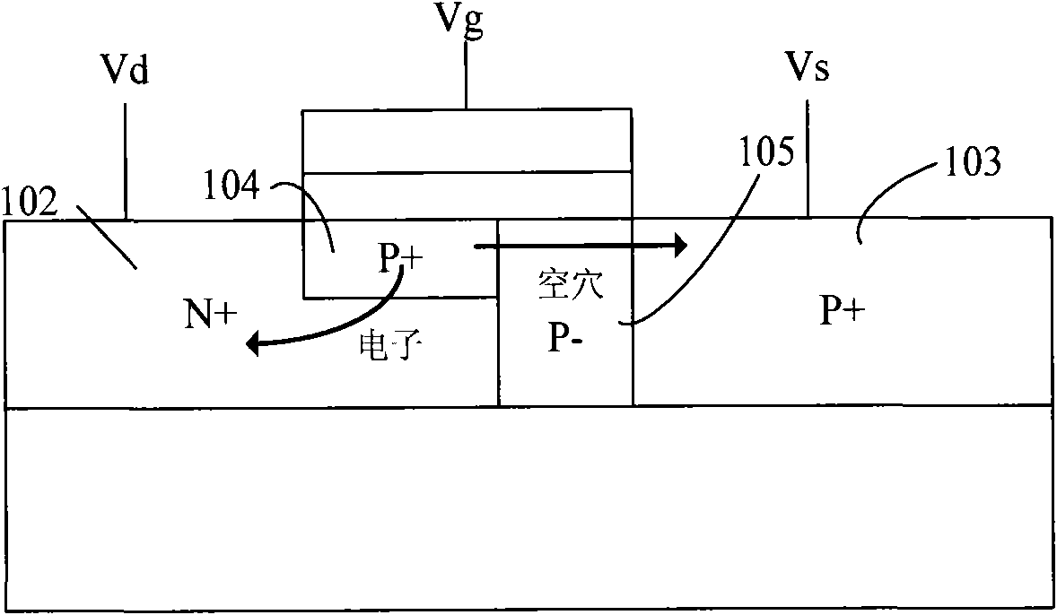
[0046] Figure 4 It is a schematic diagram of the cross-sectional structure of the green field effect transistor provided by the present invention. include:
[0047] A silicon-on-insulator 10, the silicon-on-insulator includes a silicon substrate 100, a buried oxide layer 110 and a top layer of silicon 101 sequentially located on the silicon substrate 100;
[0048] The source 1 and the drain 2 are isolated from each other and have different doping types in the top silicon layer 101;
[0049] The channel body located between the source 1 and the drain 2, the channel body is cylindrical, one end is connected to the source 1, the other end is connected to the drain 2, and it include...
PUM
 Abstract
Description
Claims
Application Information