Data processing method, device and manufacturing method for applying phosphor to LED

A technology of data processing and manufacturing methods, applied in electrical components, circuits, semiconductor devices, etc., to achieve the effect of saving resources and costs, improving utilization efficiency, and high quality

Active Publication Date: 2016-03-02
LATTICE POWER (JIANGXI) CORP
View PDF4 Cites 0 Cited by
  • Summary
  • Abstract
  • Description
  • Claims
  • Application Information

AI Technical Summary

Problems solved by technology

[0004] The first technical problem to be solved by the present invention is to provide a data processing method for applying phosphor powder to LEDs, which is used to solve the problem of accurately applying phosphor powder to each chip, so that the quality of the product remains consistent
[0005] The second technical problem to be solved by the present invention is to provide a data processing device for applying phosphor powder to LEDs, which is used to solve the problem of accurately applying phosphor powder to each chip, so that the quality of the product remains consistent
[0006] The third technical problem to be solved by the present invention is to provide a manufacturing method for applying phosphor powder to LEDs, which is used to solve the problem of accurately applying phosphor powder to each chip, so that the quality of the product remains consistent

Method used


Image

  • Data processing method, device and manufacturing method for applying phosphor to LED
  • Data processing method, device and manufacturing method for applying phosphor to LED

Examples


Embodiment Construction

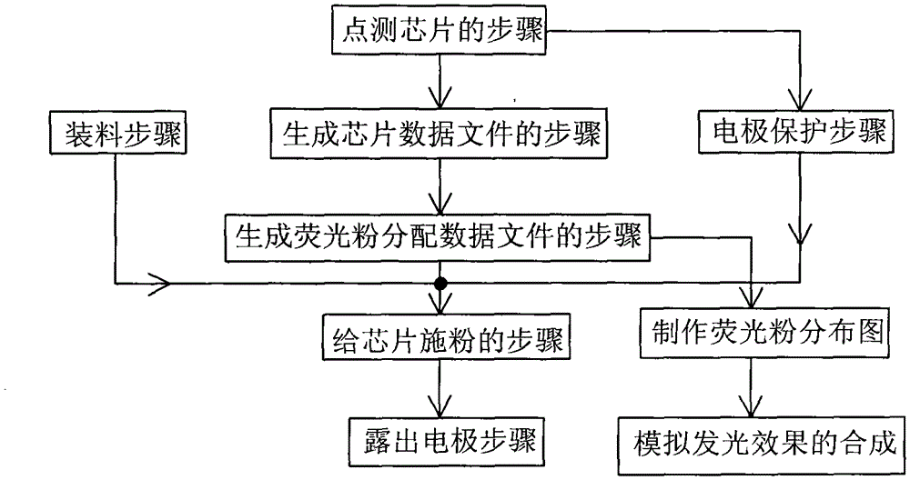
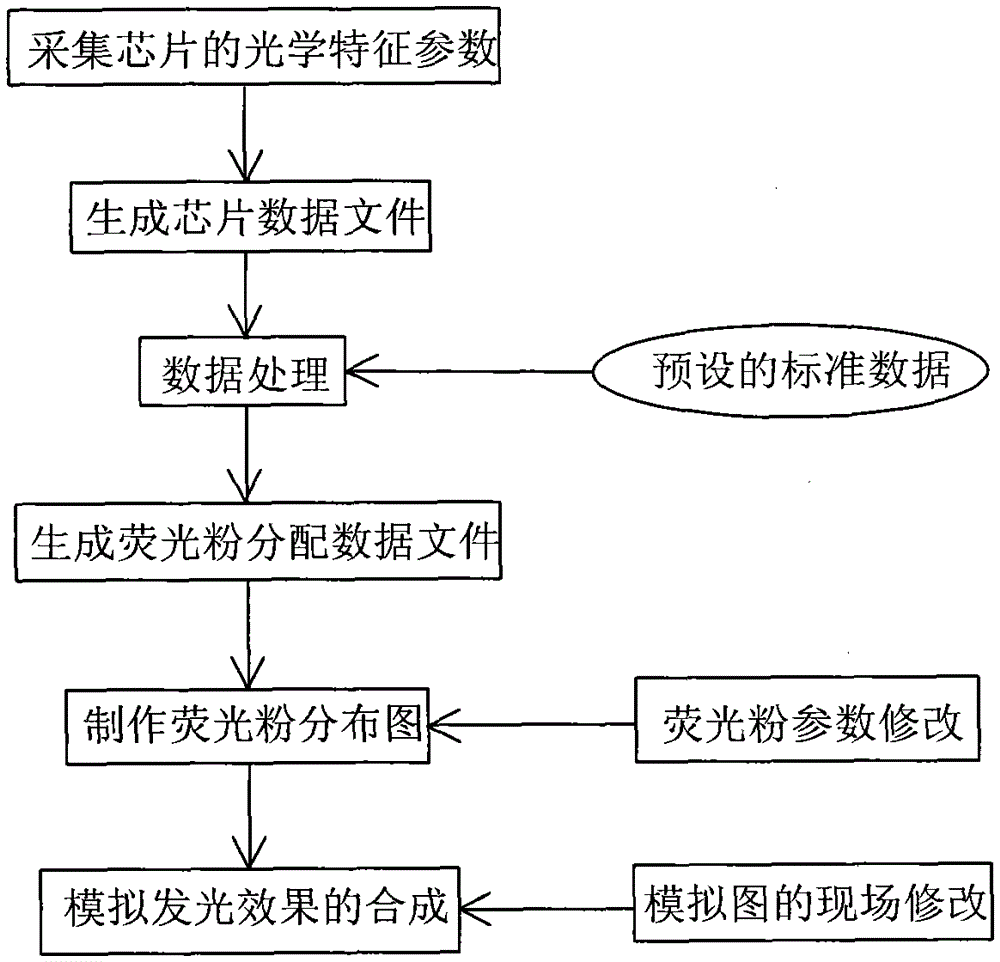
[0040] The present invention proposes a data processing method for applying fluorescent powder to LED, see figure 2 As shown, the optical characteristic parameters of the chip need to be collected before data processing. The optical characteristic parameters are mainly the main wavelength and optical power of the spot measurement output, and can also include other optical characteristic parameters, such as forward voltage, reverse breakdown voltage and lifetime. parameters etc. Then process the collected optical characteristic parameters of the chip to generate a chip data file. The chip data file can be converted into a data file directly executed by the phosphor powder application device, or a data file for further processing.

[0041]The generated chip data file is combined with the preset standard data for data processing to generate a phosphor distribution data file. The preset standard data is mainly that the chipset as a whole should have effect characteristics such a...


PUM


Abstract

The invention discloses a data processing method, device and manufacturing method for applying fluorescent powder to LEDs, which are used to solve the problem of accurately applying fluorescent powder to each chip, so as to keep product quality consistent. The technical solution of the present invention is briefly described as including the steps of generating chip data files: processing the collected optical characteristic parameters of each chip in the chipset to generate data files for system execution or further processing; generating phosphor distribution data files The step of: performing data processing on the data file, and generating a phosphor distribution data file for the amount of phosphor required for each chip according to the data in the data file. The chip product applying the technology of the invention has good consistency characteristics, more humane, more stable and more convenient processing characteristics.

Description

technical field [0001] The invention relates to a manufacturing method of a light-emitting diode, in particular to a production process of applying fluorescent powder to the light-emitting diode during the production process of the light-emitting diode. Background technique [0002] At present, in the field of semiconductor lighting, the method of realizing white light is to use the blue light emitted by InGaAlN LED to excite the YAG phosphor, and the yellow light emitted by the phosphor is synthesized with the original remaining blue light to form white light. The color coordinates of the white light of this technical solution depend on the thickness of the powder (determining how much blue light remains) and the excitation wavelength. Since epitaxy is difficult to control the uniformity of the wavelength in the chip and the consistency between the chips, and now it is common to mix the phosphor powder and the packaging material (such as silica gel), and the phosphor powder...

Claims


Application Information

Patent Timeline
Patent Type & Authority Patents(China)
IPC IPC(8): H01L33/48H01L33/50H01L33/00
Inventor 方文卿
Owner LATTICE POWER (JIANGXI) CORP
Why Eureka
Try Eureka