Method for adhering protection tape, and protection tape used in the method

A technology of protective tape and sticking roller, used in electrical components, semiconductor/solid-state device manufacturing, circuits, etc., can solve problems such as breakage, poor adsorption, and wafer falling, and achieve the effect of suppressing warpage

Inactive Publication Date: 2012-04-18
NITTO DENKO CORP
View PDF6 Cites 4 Cited by
  • Summary
  • Abstract
  • Description
  • Claims
  • Application Information

AI Technical Summary

Problems solved by technology

In this way, there is the following problem: when the wafer is subjected to backgrinding in the state where the shrinkage stress is accumulated on the protective tape, the wafer whose rigidity has been reduced due to thinning will be held by the protective tape under the contraction force of the protective tape. Warpage in the form of a concave on the bonding side (wafer front side)
[0008] After the back grinding process, the wafer with the protective tape is transported in a manner of absorbing the front side of the wafer in various subsequent processing steps, so there are also The following problems: When the wafer is concaved toward the front side and warped greatly, poor adsorption occurs, or even transportation errors occur, or the wafer falls or is damaged during transportation.

Method used


Image

  • Method for adhering protection tape, and protection tape used in the method
  • Method for adhering protection tape, and protection tape used in the method
  • Method for adhering protection tape, and protection tape used in the method

Examples


Embodiment Construction

[0055] Hereinafter, an embodiment of the present invention will be described with reference to the drawings.

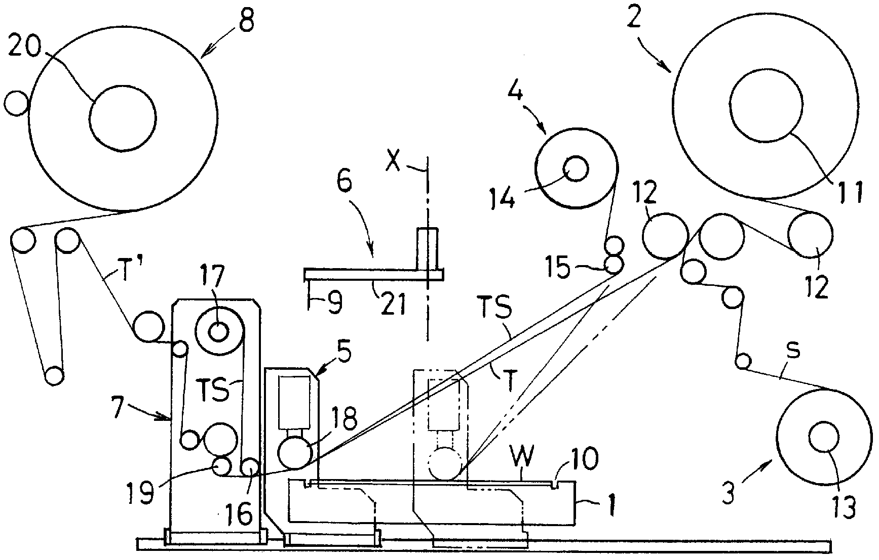
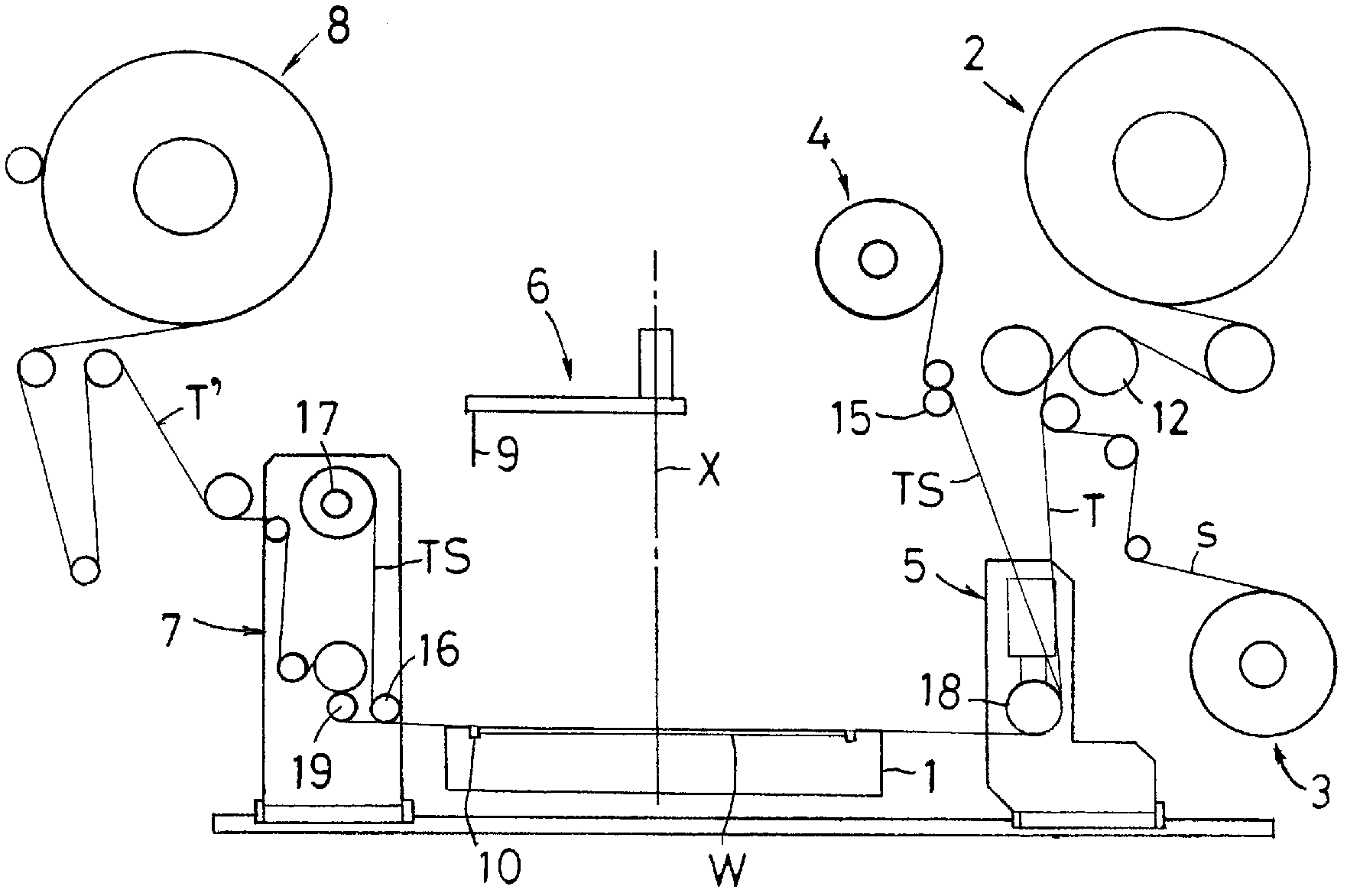
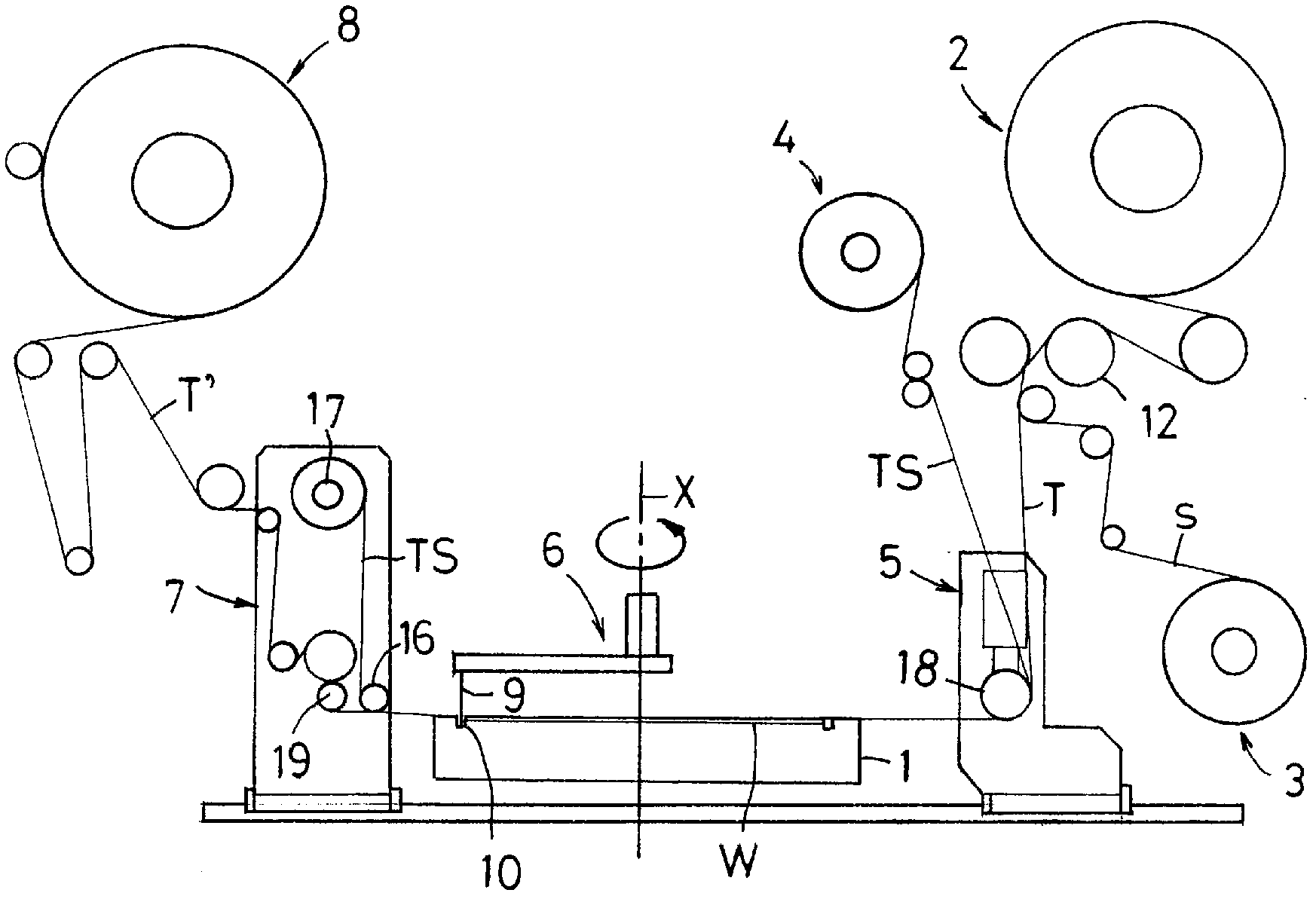
[0056] Figure 1 to Figure 4 The schematic structure of the protective tape sticking apparatus and the protective tape sticking process which carry out the method of this invention are shown in .

[0057] This protective tape sticking device has a chuck table 1 for placing and holding a semiconductor wafer W (hereinafter, simply referred to as "wafer W") by suction, and supplies wafers W held on the chuck table 1 with The tape supply unit 2 for the protective tape T for front protection, the release film recovery unit 3 that peels and recovers the release film s from the protective tape T with the release film s supplied from the tape supply unit 2, along the protective tape T The sheet supply part 4 that supplies the upper surface of the intermediate sheet TS, the sticking unit 5 that sticks the protective tape T on the wafer W sucked and held on the chuck table 1, ...


PUM


Abstract

Provided is an improved method for adhering a protection tape, by which generation of warping of a semiconductor wafer after a back-grinding step is suppressed. The protection tape (T) is supplied toward a semiconductor wafer (W) which is held on a chuck table by suction, an intermediate sheet (TS) is supplied along the upper side of the protection tape (T), and under the state wherein the intermediate sheet (TS) is disposed between an adhering member and the protection tape (T) such that the intermediate sheet can move along the surface of the base material of the protection tape (T), the adhering member and the semiconductor wafer are relatively moved horizontally, thereby adhering the protection tape (T) on the surface of the semiconductor wafer (W).

Description

technical field [0001] The present invention relates to a protective tape sticking method for sticking a protective tape on a semiconductor wafer subjected to a circuit pattern forming process, and a protective tape used in the protective tape sticking method. Background technique [0002] A semiconductor wafer (hereinafter, simply referred to as "wafer") is processed as follows. The wafer forms multiple components on its front side. In the backgrinding process, the backside of the wafer is ground. In a subsequent dicing process, the wafer is diced into individual components. In recent years, with the requirement of high-density mounting, the wafer thickness tends to be reduced from 100 μm to 50 μm, or even below 50 μm. [0003] When the wafer is thinned in the back grinding process, in order to protect the front side of the wafer on which the circuit pattern is formed, to protect the wafer from the grinding stress in the back grinding process, and to strengthen the thin ...

Claims


Application Information

Patent Timeline
Patent Type & Authority Applications(China)
IPC IPC(8): H01L21/683
CPCH01L21/67132Y10T428/2848H01L21/67706
Inventor 大牟礼智弘渡边敬介森本政和夏目雅好志村勉土生刚志山本雅之
Owner NITTO DENKO CORP
Why Eureka
Try Eureka