Method for testing shading baffle of photo-etching machine

A technology of lithography machine and light-shielding plate, which is applied in micro-lithography exposure equipment, originals for photomechanical processing, optics, etc., and can solve the problem of not being able to find out whether there is a defect in the mask plate light-shielding plate

Active Publication Date: 2014-03-12
SHANGHAI HUALI MICROELECTRONICS CORP
View PDF4 Cites 0 Cited by
  • Summary
  • Abstract
  • Description
  • Claims
  • Application Information

AI Technical Summary

Problems solved by technology

[0013] figure 1 It is a structural schematic diagram of the current industry-standard mask mask shading tape accuracy test method adopted in the background technology of the present invention, wherein, X is the horizontal direction, and Y is the longitudinal direction; figure 1 As shown, the current industry-standard test method for the accuracy of mask shading bands, that is, by adjusting the size of the mask shading plate, using exposure methods on the silicon wafer to achieve mask patterns of different sizes, and then confirming the movement accuracy of the shading plate with a microscope; Although this method can directly determine the positioning accuracy of the mask shading plate, it cannot find out whether there are defects in the manufacturing process of the mask shading plate, and whether there is light leakage in the masking plate.

Method used


Image

  • Method for testing shading baffle of photo-etching machine
  • Method for testing shading baffle of photo-etching machine
  • Method for testing shading baffle of photo-etching machine

Examples


Embodiment Construction

[0030] The specific embodiment of the present invention will be further described below in conjunction with accompanying drawing:

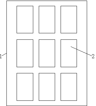
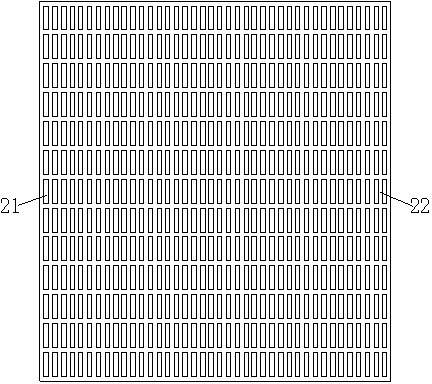
[0031] figure 2 It is a schematic diagram of the layout structure of the test image on the test template in the method for testing the shading baffle of the photolithography machine in the present invention; image 3 It is a structural schematic diagram of an enlarged test image in the method for testing the shading baffle of a photolithography machine according to the present invention. Such as figure 2 , 3 As shown, the present invention is a method for testing the shading baffle of a photolithography machine:

[0032] First, after completing the standard mask mask test, confirm that the mask mask mask has met the basic accuracy requirements.

[0033] Secondly, a binary mask (BinaryMask) or a phase shift mask (PhaseShiftMask) is used as the test mask 1, and a rectangular test image 2 is set on it, and the test image 2 consists of a plurali...


PUM

PropertyMeasurementUnit
sizeaaaaaaaaaa

Abstract

The invention relates to the field of manufacture of semiconductors and particularly relates to a method for testing a shading baffle of a photo-etching machine. According to the method provided by the invention, a test grinding plate which is provided with test graphic lines and test graphic line intervals is adopted on the basis of an industrial standard test for the shading baffle of a mask template. The test graphic line graphs arranged on the test grinding plate are highly repeated graphs and are capable of flexibly feeding back a manufacturing defect or a light-leaking problem of the shading baffle, so that a defect detecting device can be used for thoroughly testing the manufacturing defect or the light-leaking problem of the shading baffle of the mask template of the photo-etching machine after the test graphic line graphs are exposed on a silicon wafer.

Description

technical field [0001] The invention relates to the field of semiconductor integrated circuits and its manufacture, in particular to a method for testing a shading baffle of a photolithography machine. Background technique [0002] With the continuous improvement of integrated circuit manufacturing technology, the area of ​​semiconductor devices is becoming smaller and smaller, and the layout of semiconductors has evolved from an ordinary single-function separation device to an integrated high-density multi-functional integrated circuit; it has changed from the original integrated circuit (Integrated Circuit, referred to as IC) has gradually evolved into a large-scale integrated circuit (LargeScaleIntegratedcircuit, referred to as LSI), very large-scale integrated circuit (Very LargeScaleIntegratedCircuit, referred to as VLSI), until now ultra-large-scale integrated circuit (UltraLargeScaleIntegration, referred to as ULSI), the area of ​​the semiconductor device is getting mo...

Claims


Application Information

Patent Timeline
Patent Type & Authority Patents(China)
IPC IPC(8): G03F7/20G03F1/44
Inventor 朱骏陈力钧郑刚
Owner SHANGHAI HUALI MICROELECTRONICS CORP
Why Eureka
Try Eureka