Optical fiber array for directly coupling with array VSCEL (vertical cavity surface emitting laser) or PD (photoelectric detector) chip and manufacturing method thereof

An optical fiber array and manufacturing method technology, applied in the field of optical fiber products, can solve problems affecting coupling efficiency and ease of use, etc.

Active Publication Date: 2014-11-05
SHENZHEN GIGALIGHT TECH
View PDF3 Cites 1 Cited by
  • Summary
  • Abstract
  • Description
  • Claims
  • Application Information

AI Technical Summary

Problems solved by technology

At this time, the axial direction of the optical fiber is 90 degrees to the direction of light emitted by the laser array or the direction of light received by the detector. Use a 45° reflection angle to reflect and couple the laser light emitted by the VCSEL chip of the laser array into the optical fiber or deflect the optical fiber transmission beam by 90° ° irradiates the photosensitive surface of the array detector, but because the optical fiber forms a complete 45° plane with the grooved substrate and the glass gland, and the optical fiber is sandwiched between the grooved substrate and the glass gland, the grooves on the upper and lower sides The substrate and the glass cover will form a barrier to the emitted laser beam or the received laser beam, thus affecting the coupling efficiency and ease of use

Method used


Image

  • Optical fiber array for directly coupling with array VSCEL (vertical cavity surface emitting laser) or PD (photoelectric detector) chip and manufacturing method thereof
  • Optical fiber array for directly coupling with array VSCEL (vertical cavity surface emitting laser) or PD (photoelectric detector) chip and manufacturing method thereof
  • Optical fiber array for directly coupling with array VSCEL (vertical cavity surface emitting laser) or PD (photoelectric detector) chip and manufacturing method thereof

Examples


Embodiment Construction

[0032] In order to make the above objects, features and advantages of the present invention more comprehensible, specific implementations of the present invention will be described in detail below in conjunction with the accompanying drawings. In the following description, numerous specific details are set forth in order to provide a thorough understanding of the present invention. However, the present invention can be implemented in many other ways different from those described here, and those skilled in the art can make similar improvements without departing from the connotation of the present invention, so the present invention is not limited by the specific implementations disclosed below.

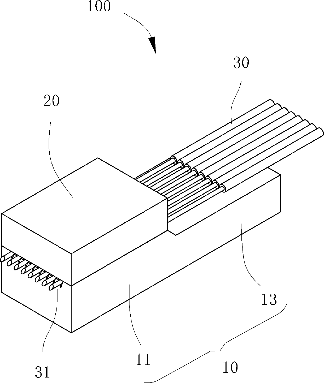
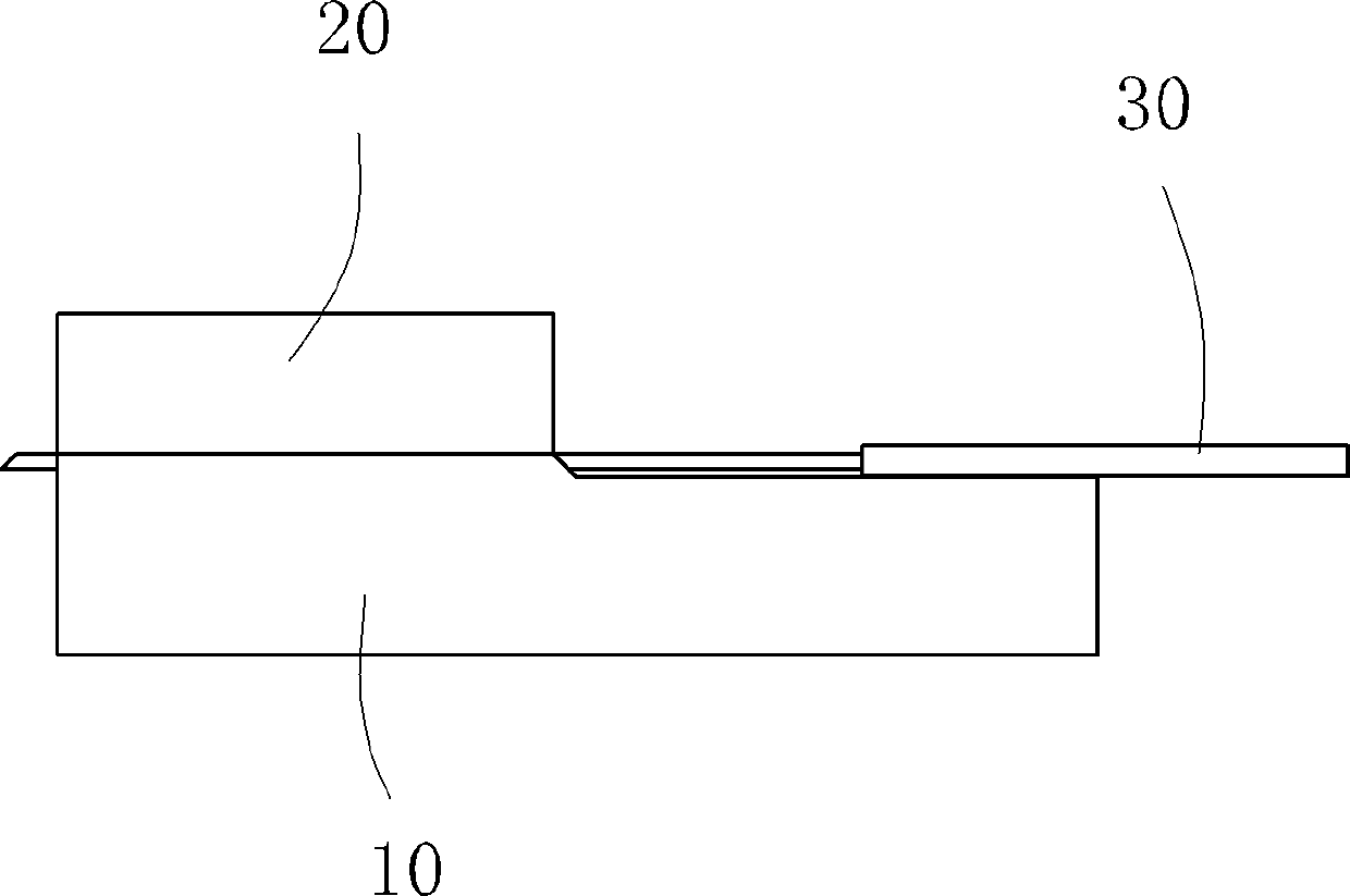
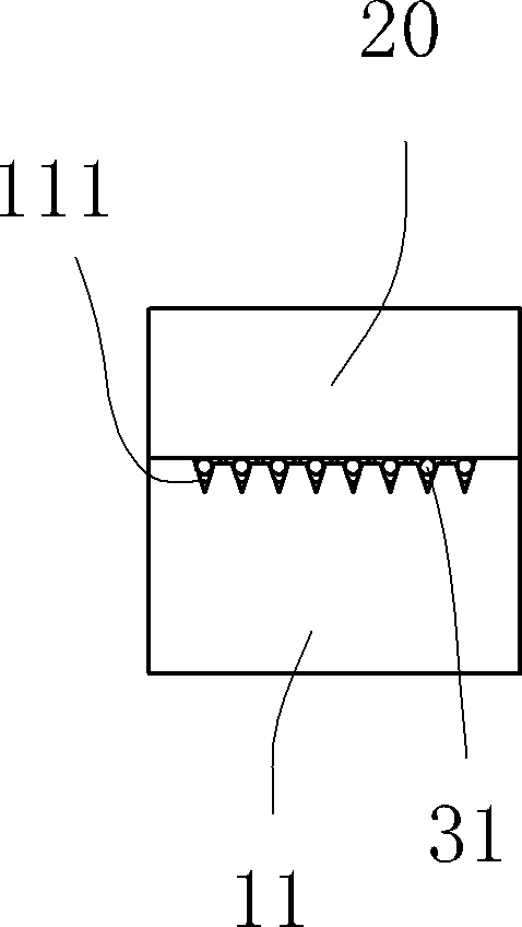
[0033] see Figure 1 to Figure 4 , the optical fiber array 100 of the first embodiment is mainly used for direct coupling with the array VCSEL or PD chip, which includes a grooved substrate 10, a gland substrate 20, and is sandwiched between the grooved substrate 10 and the gland subs...


PUM


Abstract

The invention relates to an optical fiber array for directly coupling with an array VSCEL (vertical cavity surface emitting laser) or PD (photoelectric detector) chip. The optical fiber array comprises a groove substrate, a gland substrate and an optical fiber belt clamped between the groove substrate and the gland substrate, wherein an end part of the optical fiber belt is protruded out of a plane jointly defined by the end face of the groove substrate and the end face of the gland substrate; and the end face of the optical fiber belt is an optical plane with a 45-degree inclined angle. When the optical fiber array is directly coupled with an optical waveguide integrated device, each optical fiber core is easily aligned with each pixel of the optical waveguide integrated device during the use process, the coupling operation is more convenient and the coupling efficiency is higher, because the end part of the optical fiber belt is ground and processed as a 45-degree optical plane according to the requirement and completely extends for an enough distance outside the end face of the optical fiber array and the obstruction of the groove substrate and the gland substrate on upper and lower sides to the laser beam is eliminated. The invention also provides a manufacturing method for the optical fiber array.

Description

【Technical field】 [0001] The invention relates to an optical fiber product, in particular to an optical fiber array for direct coupling with an array VCSEL or PD chip and a manufacturing method thereof. 【Background technique】 [0002] Traditional optical fiber arrays are generally composed of substrates including grooves (usually V-shaped grooves or U-shaped grooves), glass gland substrates, and optical fiber ribbons between them, which are bonded by adhesives. An optical fiber component used to transmit laser energy produced by grinding process. The grooved substrate of the optical fiber array is usually made of quartz glass, borosilicate glass or silicon material. [0003] When the fiber array is directly coupled with the parallel emitting laser array VCSEL (Vertical Cavity Surface Emitting Laser) chip or photodetector (PD) chip, each fiber core of the fiber array is connected to each parallel emitting laser array chip. The pixel or array detector PIN (or GaAs) chip is al...

Claims


Application Information

Patent Timeline
Patent Type & Authority Patents(China)
IPC IPC(8): G02B6/43
Inventor 邱锦和
Owner SHENZHEN GIGALIGHT TECH
Why Eureka
Try Eureka