
Using interrupted through-silicon-vias in integrated circuits adapted for stacking

A technology of integrated circuits and vias, applied in circuits, electrical components, electronic switches, etc., to solve the problems of indistinguishable chips and power loss.

Inactive Publication Date: 2012-07-11
CONVERSANT INTPROP MANAGEMENT INC
View PDF12 Cites 11 Cited by
  • Summary
  • Abstract
  • Description
  • Claims
  • Application Information

AI Technical Summary

Problems solved by technology

However, the problem in stacking bus memory chips is that each chip is indistinguishable
However, if all stacked storage units are the same, the last unit will have an input to the controller not connected to the downstream link
These unconnected inputs pick up random noise, causing unnecessary logic transitions on each downstream link, resulting in unnecessary power loss

Method used


Image

  • Using interrupted through-silicon-vias in integrated circuits adapted for stacking
  • Using interrupted through-silicon-vias in integrated circuits adapted for stacking
  • Using interrupted through-silicon-vias in integrated circuits adapted for stacking

Examples


Embodiment Construction

[0024] Exemplary embodiments of the present invention use discontinuous TSVs that provide series connection through successive integrated circuit die in a stack without the need to rotate the die. With discontinuous TSVs, the connection between the bottom and top pads is broken to allow connections other than direct (non-discontinuous) vertical connections.

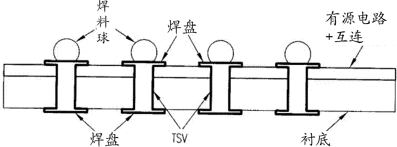
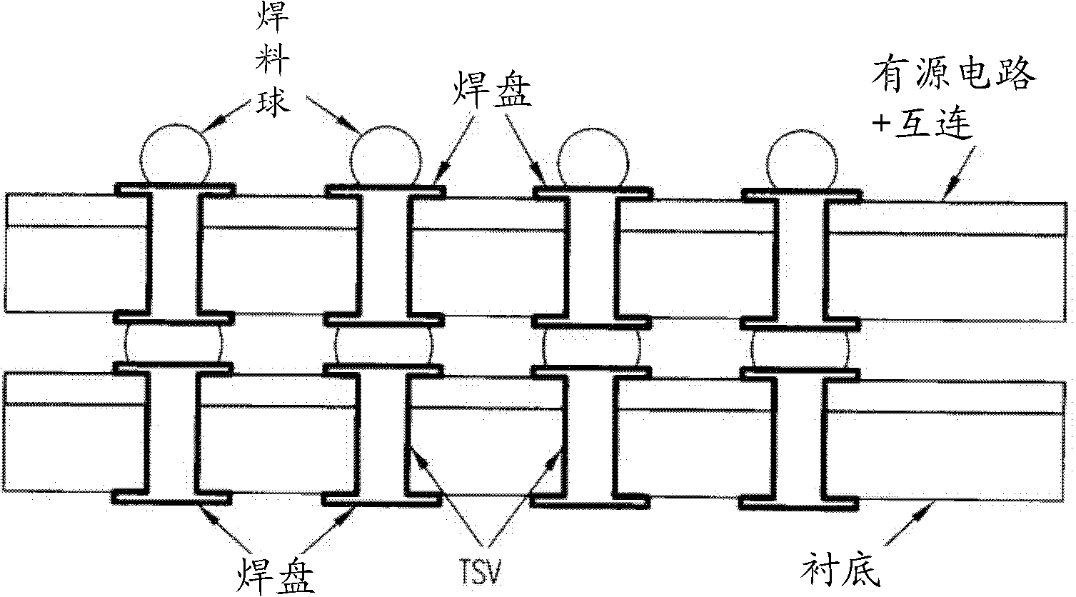
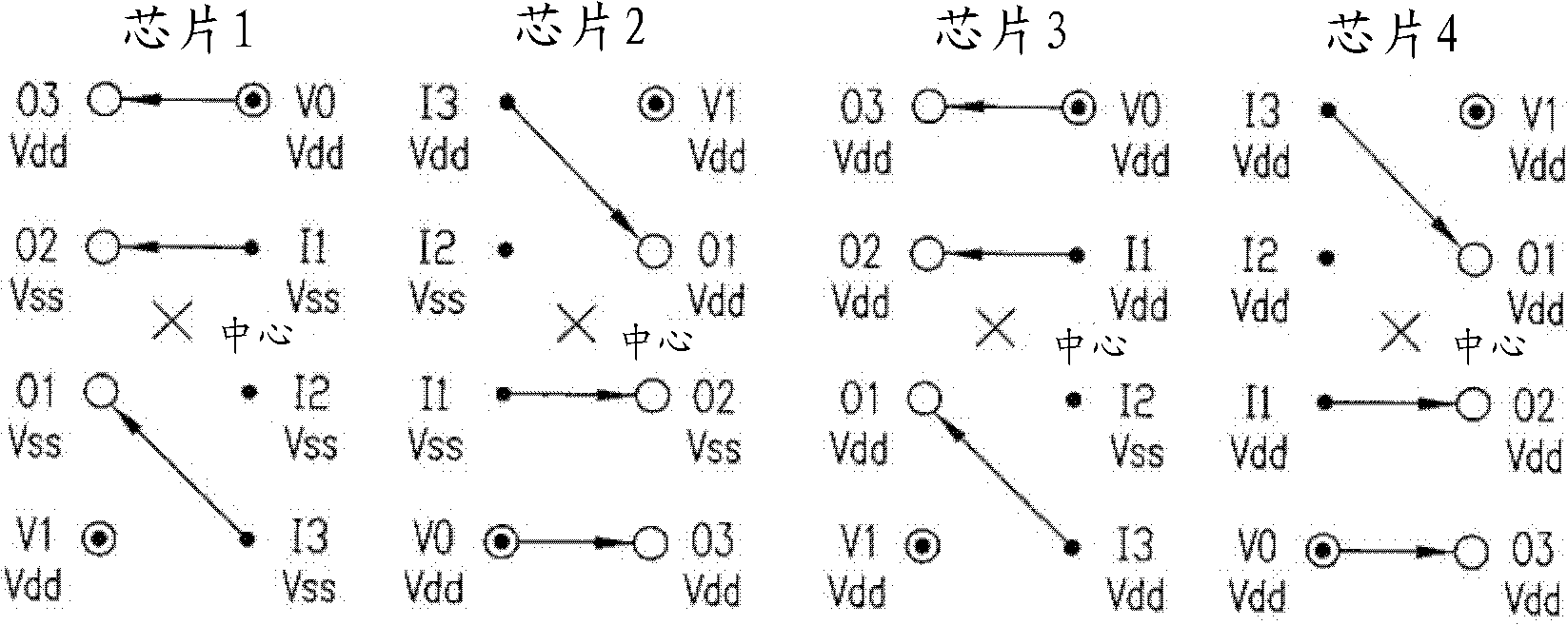
[0025] image 3 An example of stacked chips interconnected with discontinuous TSVs according to the invention is shown, which provides connections that are not direct vertical connections. The TSVs at A are conventional non-interrupted vertical connections between pads on the bottom surface of the die and the top metal layer, and the TSVs at B, C, and D are interrupted TSVs.

[0026] There are multiple conductive layers within the active circuitry and interconnect areas of the chip. Current logic processes have 9 or more layers of metal interconnects. The top metal layer is denoted here as metal n and the bottom layer ...


PUM


Abstract

In an integrated circuit (IC) adapted for use in a stack of interconnected ICs, interrupted through-silicon-vias (TSVs) are provided in addition to uninterrupted TSVs. The interrupted TSVs provide signal paths other than common parallel paths between the ICs of the stack. This permits IC identification schemes and other functionalities to be implemented using TSVs, without requiring angular rotation of alternate ICs of the stack.

Description

[0001] related application [0002] This application claims priority to co-pending U.S. Provisional Patent Application Serial No. 61 / 239,211 filed September 2, 2009 and U.S. Patent Application Serial No. 12 / 757,540 filed April 9, 2010 right, the entire contents of which are hereby incorporated by reference. technical field [0003] The present invention relates generally to integrated circuits, and more particularly to stacked arrangements of interconnected integrated circuits. Background technique [0004] Through silicon via (TSV) technology is an emerging method for connecting stacked semiconductor integrated circuit (IC) chips. Because the density of TSVs can be much higher than that of conventional pads for wire bonding, very wide buses can be achieved. Conventional bonding pads for wire bonding have a planar size of about 100um, while TSVs may be 10um or even smaller. Because the connections between each chip in the chip stack are made vertical, the busses between ...

Claims


Application Information

Patent Timeline
Patent Type & Authority Applications(China)
IPC IPC(8): H01L23/488H01L21/71H01L21/98H01L23/50H03K17/56G11C5/06
CPCH01L21/02697H01L23/544G11C5/02H01L2225/06562H01L23/5286H01L21/82H01L25/0657H01L24/03H01L2223/5444H01L2223/54433H01L2225/06527H01L2225/06541H01L2224/06181H01L2924/01055H01L2224/0401H01L2225/06513H01L23/481H01L2924/01078G11C5/06H03K17/00H01L24/16H01L2924/14H01L2924/00H01L23/488H01L23/50H01L2225/0652H01L2225/06548
Inventor P·B·吉灵厄姆
Owner CONVERSANT INTPROP MANAGEMENT INC
Learn More