Method for manufacturing organic electroluminescent element, organic electroluminescent element, display device and illuminating device

A technology of electroluminescent devices and manufacturing methods, which is applied in the direction of electroluminescent light sources, lighting devices, semiconductor/solid-state device manufacturing, etc., can solve problems such as damage, incorporation, and deterioration, and achieve high driving stability, long driving life, The effect of low manufacturing cost

Active Publication Date: 2012-08-29
MITSUBISHI RAYON CO LTD
View PDF30 Cites 3 Cited by
  • Summary
  • Abstract
  • Description
  • Claims
  • Application Information

AI Technical Summary

Problems solved by technology

[0010] On the other hand, the organic layers constituting the organic electroluminescent device formed by the wet film-forming method, especially the light-emitting functional materials contained in these organic layers, etc. will cause damage due to contact with moisture in the air, oxygen, ozone, etc. deterioration (damage)
Furthermore, there is also a possibility that impurities in the atmosphere may be adsorbed and mixed in on the surface of the membrane (Patent Documents 4 and 5)

Method used


Image

  • Method for manufacturing organic electroluminescent element, organic electroluminescent element, display device and illuminating device
  • Method for manufacturing organic electroluminescent element, organic electroluminescent element, display device and illuminating device
  • Method for manufacturing organic electroluminescent element, organic electroluminescent element, display device and illuminating device

Examples


Embodiment 1)

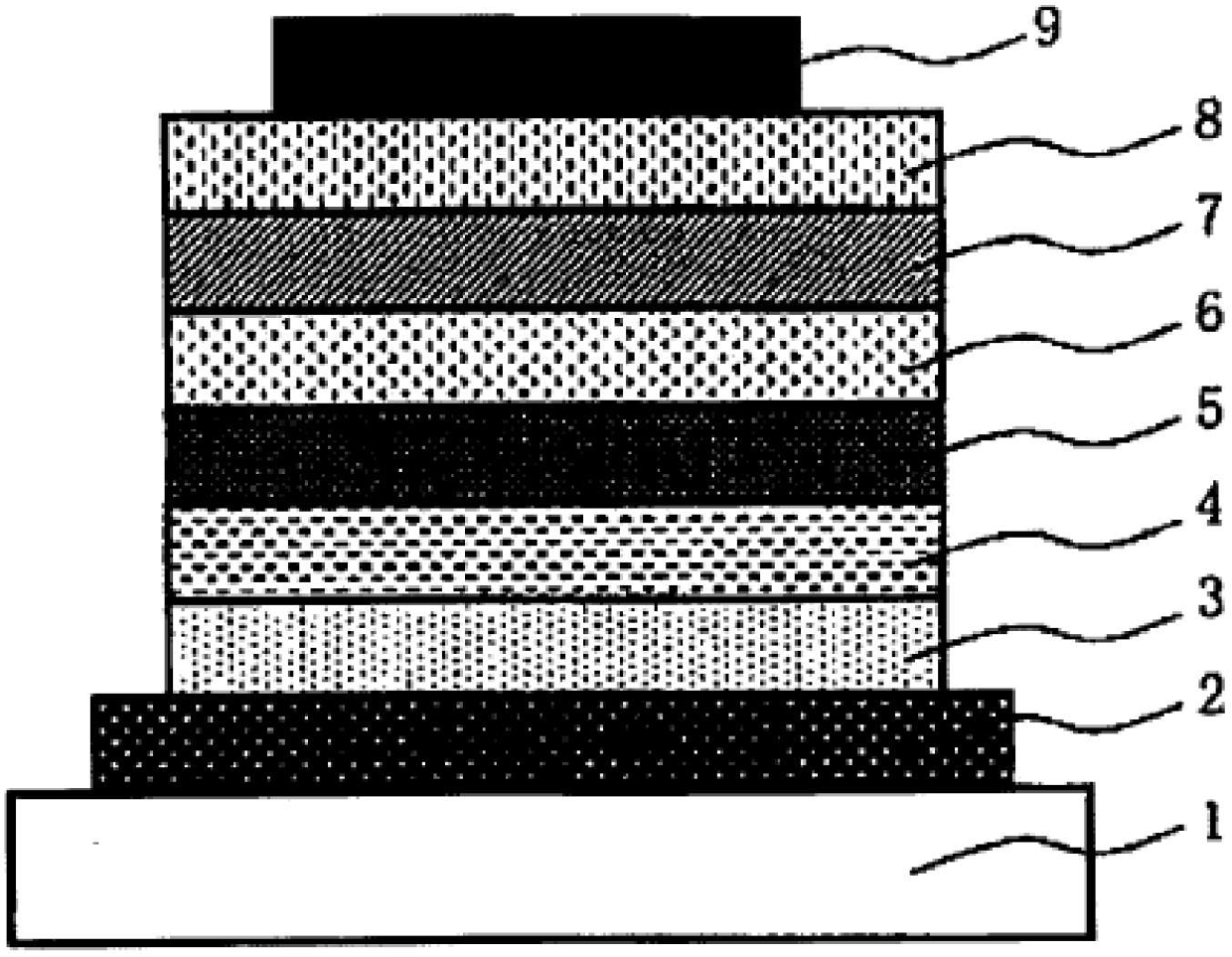
[0340] Made with figure 1 The organic electroluminescence device of the structure shown.

[0341] A product obtained by depositing an indium-tin oxide (ITO) transparent conductive film at a thickness of 150 nm on a glass substrate 1 (sputtered film product; sheet resistance 15 Ω) is patterned to a thickness of 2 mm using usual photolithography techniques and hydrochloric acid etching. The anode 2 is formed in a wide stripe shape. The patterned ITO substrate was cleaned in the order of ultrasonic cleaning with acetone, water washing with pure water, and ultrasonic cleaning with isopropanol, then dried with nitrogen gas, and finally ultraviolet ozone cleaning was performed.

[0342] Next, the hole injection layer 3 was formed by the following wet film-forming method. A charge transport material having an aromatic amino group (PB-1 (weight average molecular weight: 52000, number average molecular weight: 32500)) with the following structural formula and an electron-accepting c...

Embodiment 2)

[0380] Using the compound (HO-2) of the following structural formula instead of the organic compound (HO-1) as the material of the light-emitting layer, spin-coating was performed under the same conditions, and the organic electroluminescence was produced in the same manner as in Example 1. Light emitting devices.

[0381] Among them, a uniform thin film (light-emitting layer) with a film thickness of 40 nm was formed by spin coating.

[0382]

reference example 1)

[0384] Using the compound (HO-3) of the following structural formula instead of the organic compound (HO-1) as the material of the light-emitting layer, spin-coating was performed under the same conditions, and the organic electroluminescence was produced in the same manner as in Example 1 Light emitting devices.

[0385] Among them, a uniform thin film (light-emitting layer) with a film thickness of 40 nm was formed by spin coating.

[0386]


PUM

PropertyMeasurementUnit
thicknessaaaaaaaaaa
boiling pointaaaaaaaaaa
thicknessaaaaaaaaaa

Abstract

Disclosed is an organic electroluminescent element which has high driving stability and long service life. The organic electroluminescent element can be produced at low cost by forming a light-emitting layer using a composition for light-emitting layer formation in a specific environment, said composition containing a solvent and a compound that has a specific structure. Specifically disclosed is a method for manufacturing an organic electroluminescent element that comprises a light-emitting layer between a first electrode and a second electrode that is formed so as to face the first electrode. The method for manufacturing an organic electroluminescent element is characterized by comprising a light-emitting layer formation step wherein a coating film is formed by a wet film-forming process using a composition for light-emitting layer formation in an environment having an oxygen concentration of 18-22% by volume, said composition containing a solvent and a compound that is represented by general formula (1) and has a molecular weight of not less than 400. (In general formula (1), Ar31 and Ar32 each independently represents a substituted aromatic hydrocarbon ring group or an aromatic heterocyclic group. In this connection, a compound represented by general formula (1) does not have a partial structure of a nitrogen atom-containing heterocycle.)

Description

technical field [0001] The present invention relates to a manufacturing method of an organic electroluminescent device with high luminous efficiency and driving stability, an organic electroluminescent device manufactured by the manufacturing method, and a display device and an illuminating device having the organic electroluminescent device. Background technique [0002] In recent years, development of electroluminescent devices (organic electroluminescent devices) using organic thin films is underway. Examples of the method for forming the organic thin film include a vacuum vapor deposition method and a wet film-forming method. Among them, the wet film-forming method has the advantages of not requiring vacuum treatment, being easy to enlarge the area, and easily mixing and adding various materials with various functions in one layer (coating liquid). [0003] Polymer materials such as poly(p-phenylene vinylene) derivatives and polyfluorene derivatives are mainly used as m...

Claims


Application Information

Patent Timeline
Patent Type & Authority Applications(China)
IPC IPC(8): H05B33/10C09K11/06H01L51/50C07D215/30C07D307/91C07D401/10
CPCC07D215/30C07D307/91C07D401/14C07D403/14C09K11/06C09K2211/1011C09K2211/1014H05B33/10H05B33/14H10K71/12H10K71/811H10K85/115H10K85/151H10K85/626H10K85/633H10K85/342H10K50/11
Inventor 鹤谷泰之佐藤秀树今田一郎
Owner MITSUBISHI RAYON CO LTD
Why Eureka
Try Eureka