Method and device for working condition management on dual-interface smart card chip

A dual-interface smart card, working state technology, applied in the field of smart cards, can solve the problem that the performance of dual-interface smart card chips is limited by the working state of SRAM

Active Publication Date: 2012-11-28
DATANG MICROELECTRONICS TECH CO LTD
View PDF3 Cites 2 Cited by
  • Summary
  • Abstract
  • Description
  • Claims
  • Application Information

AI Technical Summary

Problems solved by technology

[0004] The invention provides a method and device for managing the working state of a dual-interface smart card chip, which solves the problem that the performance of the dual-interface smart card chip is limited by the working state of the SRAM

Method used


Image

  • Method and device for working condition management on dual-interface smart card chip
  • Method and device for working condition management on dual-interface smart card chip
  • Method and device for working condition management on dual-interface smart card chip

Examples


Embodiment Construction

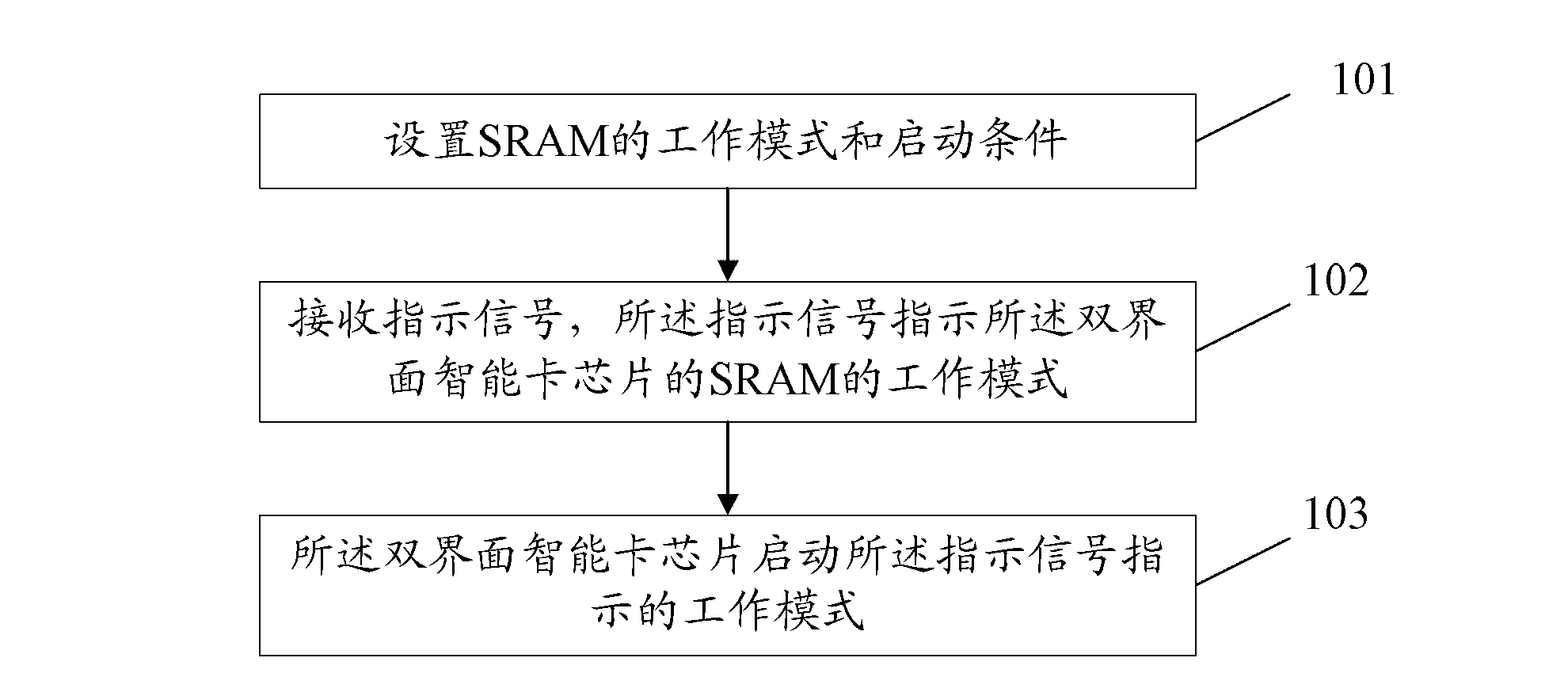
[0032] The disadvantages of the prior art are: if you want to reduce the average current and peak current of the SRAM, you must reduce the working speed of the SRAM; if you want to increase the working speed of the SRAM, the average current and peak current will increase accordingly, increasing Power consumption on SRAM. The two restrict each other, so that the working speed of SRAM cannot reach high speed, and its peak current cannot be reduced to a relatively low level, thus restricting the performance of dual-interface smart card chips.

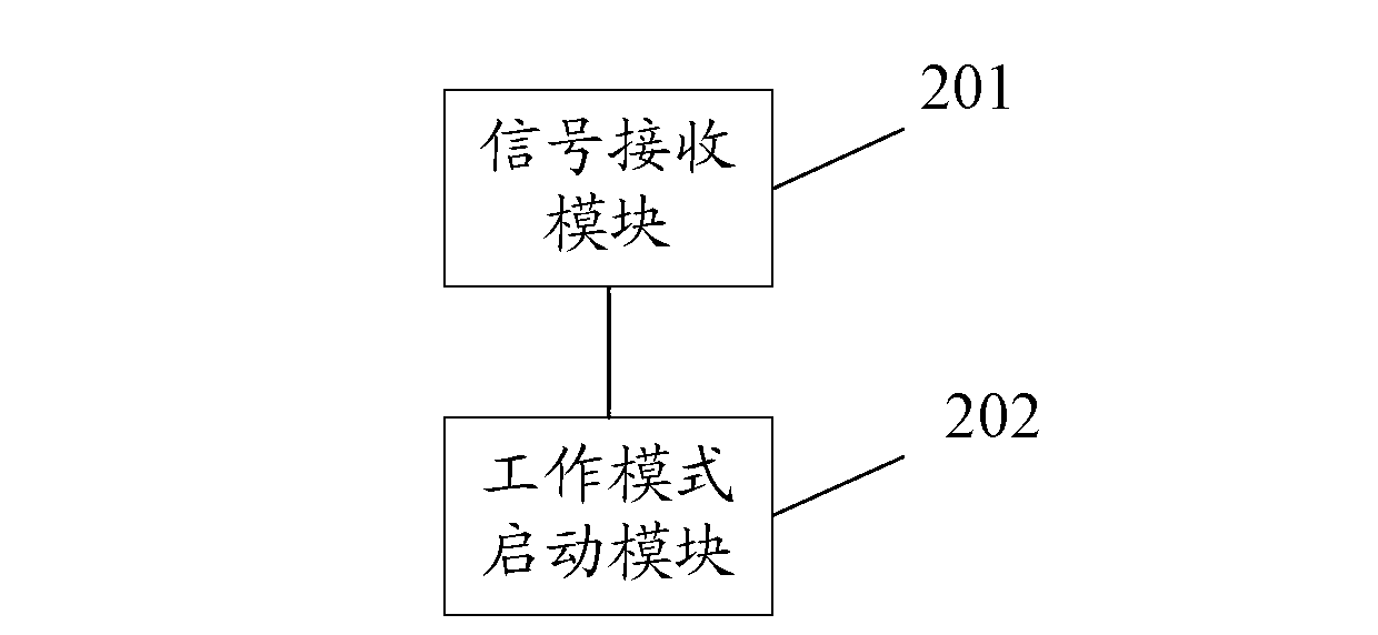
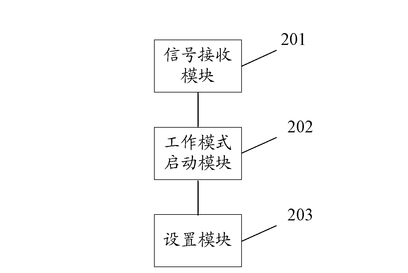
[0033] In order to solve the above problems, the present invention provides a dual-interface smart card chip working state management method. Hereinafter, the embodiments of the present invention will be described in detail with reference to the accompanying drawings. It should be noted that the embodiments in the application and the features in the embodiments can be combined with each other arbitrarily if there is no conflict.

[0034] Firs...


PUM


Abstract

The invention provides a method and a device for working condition management on a dual-interface smart card chip, relates to the field of smart cards, and solves the problem that the performance of the dual-interface smart card chip is limited by the working condition of a SRAM (Static Random Access Memory). The method comprises the following steps that: the dual-interface smart card chip receives an indication signal, wherein the indication signal indicates the work mode of the SRAM of the dual-interface smart card chip; and the dual-interface smart card chip starts the work mode indicated by the indication signal. The technical scheme provided by the invention is suitable for the dual-interface smart card with a contact type port and a non-contact type port, and realizes switching control on the work mode of the SRAM.

Description

Technical field [0001] The invention relates to the field of smart cards, in particular to a method and device for managing the working state of a dual-interface smart card chip. Background technique [0002] In the dual-interface smart card chip, the contact interface requires SRAM to run at high speed, and the data read and write speed is fast. Such a static random access memory (SRAM) has a very large average current and peak current; while the contactless interface works alone At this time, since the energy of the entire chip is coupled through the antenna, the energy obtained is limited, and it is required that the average current and peak current of the SRAM cannot be large when it is running, so as to meet the requirements of low power consumption, but the requirements for speed are on the middle. There is a contradiction between high speed and low power consumption. In this way, the SRAM high speed and low current in the dual interface card chip cannot be satisfied at the...

Claims


Application Information

Patent Timeline
Patent Type & Authority Applications(China)
IPC IPC(8): G06F3/06
Inventor 张祥杉李紫金
Owner DATANG MICROELECTRONICS TECH CO LTD
Why Eureka
Try Eureka