Detection device of printed circuit board

A technology for printed circuit boards and inspection devices, applied to measuring devices, material analysis through optical means, instruments, etc., can solve the problem of not being able to detect edge shapes smoothly

Inactive Publication Date: 2013-03-06
玛机统丽公司
View PDF8 Cites 8 Cited by
  • Summary
  • Abstract
  • Description
  • Claims
  • Application Information

AI Technical Summary

Problems solved by technology

[0003] However, when an image of a printed circuit board is obtained by such an inspection device, when light is irradiated from a direction that is regular reflection with respect to the camera (that is, bright field illumination), the light is strongly affected by edges, corners of uneven parts, and the like. reflection, the shape of the edge cannot be detected smoothly

Method used


Image

  • Detection device of printed circuit board
  • Detection device of printed circuit board
  • Detection device of printed circuit board

Examples


Embodiment Construction

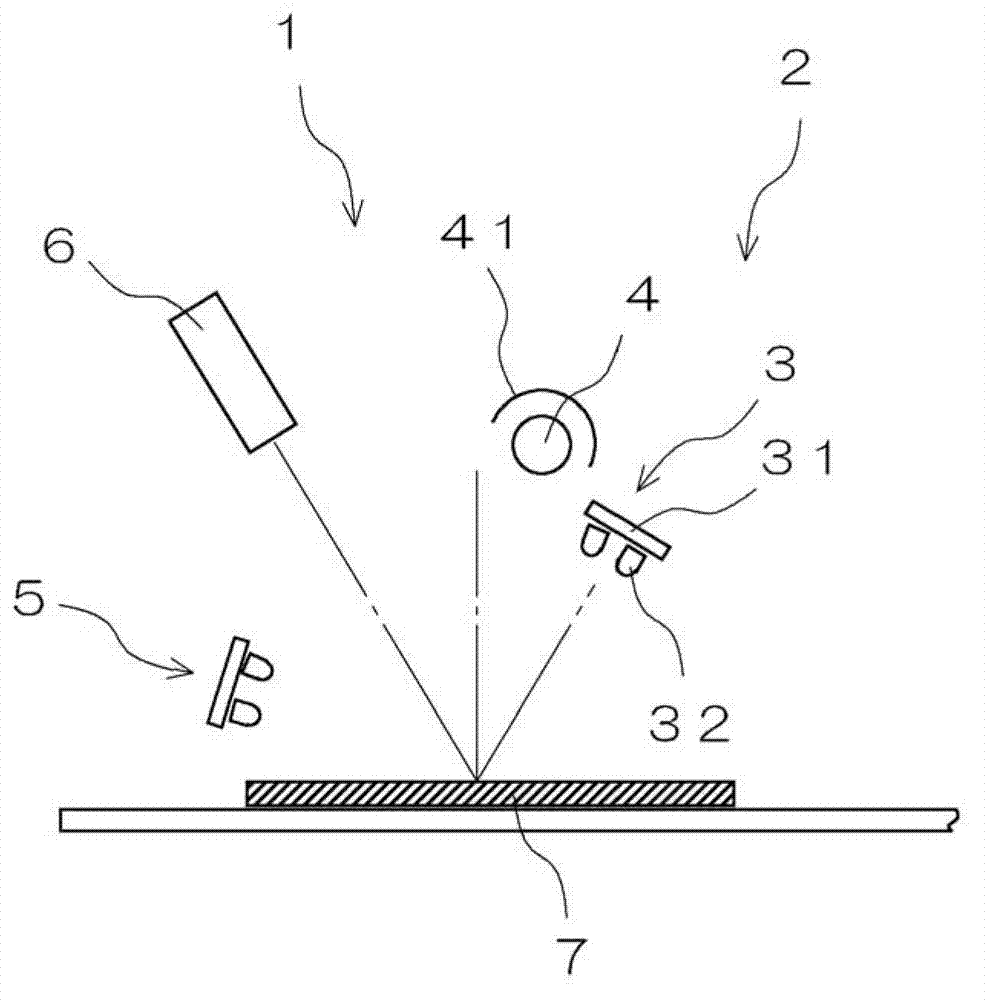
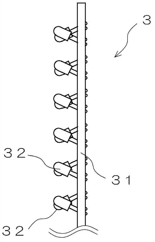
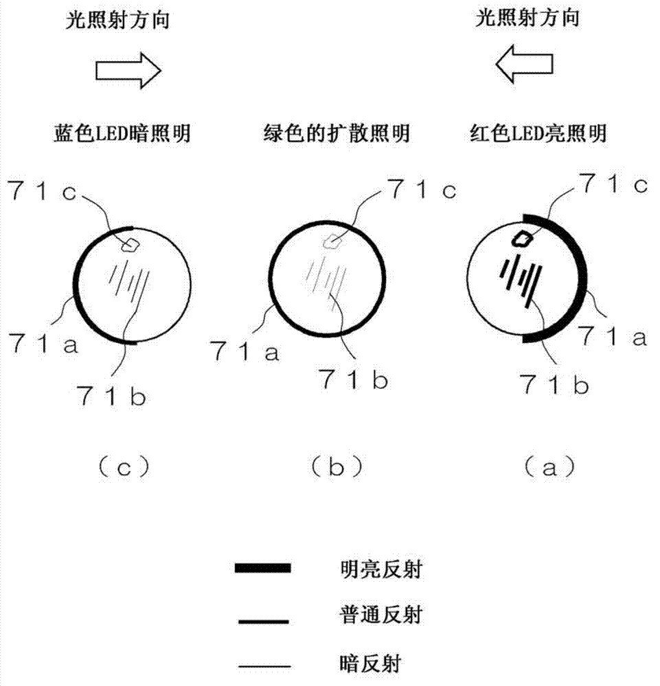
[0032] Hereinafter, an embodiment of the present invention will be described with reference to the drawings. The inspection device 1 for a printed circuit board 7 of this embodiment is configured to include: an illuminating device 2 that irradiates light to a printed circuit board 7 placed on a table; The camera 6 of reflected light; the first inspection unit 81 to the third inspection unit 83 for inspecting the formation state of the pad 71, the resist 72, etc. formed on the surface of the printed circuit board 7 based on the image obtained by the camera 6 (refer to Image 6 )Wait. Furthermore, the lighting device 2 is characterized in that it includes a first color light source 3 including a red LED 32 disposed at a first angle of regular reflection with respect to the optical axis of the camera 6 (that is, at an angle for bright field illumination). ; be configured as a green fluorescent lamp at an angle different from the first angle, that is, a second color light source...


PUM


Abstract

A detection device of a printed circuit board radiates light corresponding to the characteristics of the objects, such as pad, resist, etc., to carry out a detection of excellent precision. The detection device (1) of the printed circuit board (7) is equipped with a red LED (32) configured to be a bright field illumination first angle relative to a camera (6); a second color light source (4) which is an illumination carried out by a green fluorescent lamp, and a third color light source (5) composed of a blue LED configured as a dark field illumination third angle relative to the camera (6). The light of the first and third color light sources (3,5) is used and the camera (6) is used to shoot the image of the printed circuit board (7), and the image generated by the light come from a red LED (32) as the bright field illumination is used to detect whether the scar (71b) and concave scar (71c) on the surface of the pad are discolored; in addition, the image generated by the light come from a fluorescent lamp as a green diffused illumination is utilized to detect the formation state of the outline (71a) of the pad (71), so that the image come from a blue LED, namely the third color light source (5), is used to detect the accumulation and defect of the resist and in addition, the situations, such as pattern broken line, short circuit, etc., below the resist.

Description

technical field [0001] The present invention relates to an inspection device for a printed wiring board capable of accurately inspecting pads, resist, and the like formed on the surface of the printed wiring board. Background technique [0002] Usually, a camera acquires images of pads, resists, and the like formed on the surface of a printed wiring board, and inspections are automatically performed based on the images. [0003] However, when an image of a printed circuit board is obtained by such an inspection device, when light is irradiated from a direction that is regular reflection with respect to the camera (that is, bright field illumination), the light is strongly affected by edges, corners of uneven parts, and the like. reflection, the shape of the edge cannot be detected smoothly. Therefore, generally, when acquiring an image of a printed circuit board, the image is acquired under dark-field illumination in which light is irradiated from a direction different from...

Claims


Application Information

Patent Timeline
Patent Type & Authority Applications(China)
IPC IPC(8): G01N21/95G01N21/956
CPCG01N21/956G01N2021/95638G01N2201/0627G01N2021/8825
Inventor 笹井昌年
Owner 玛机统丽公司
Why Eureka
Try Eureka