Eureka AIR delivers breakthrough ideas for toughest innovation challenges, trusted by R&D personnel around the world.

Semiconductor memory device having three-dimensionally arranged resistive memory cells

A semiconductor and memory technology, applied in the field of semiconductor storage devices, can solve the problems of high cost of pattern miniaturization technology, limited increase in number of bits, etc.

Inactive Publication Date: 2013-06-05
SAMSUNG ELECTRONICS CO LTD
View PDF1 Cites 8 Cited by
  • Summary
  • Abstract
  • Description
  • Claims
  • Application Information

AI Technical Summary

Problems solved by technology

However, the use of pattern miniaturization technology will be limited due to high cost, and the capacity increase achieved by MLC technology will be limited by the number of bits to be increased in each cell

Method used


Image

  • Semiconductor memory device having three-dimensionally arranged resistive memory cells
  • Semiconductor memory device having three-dimensionally arranged resistive memory cells
  • Semiconductor memory device having three-dimensionally arranged resistive memory cells

Examples


Embodiment Construction

[0051] Example embodiments of inventive concepts will now be described more fully with reference to the accompanying drawings, in which some example embodiments are shown. Example embodiments of inventive concepts may, however, be embodied in many different forms and should not be construed as limited to the embodiments set forth herein; The ideas are fully conveyed to those skilled in the art. In the drawings, the thicknesses of layers and regions are exaggerated for clarity. The same reference numerals in the drawings denote the same elements, and thus descriptions thereof will be omitted.

[0052] It will be understood that when an element is referred to as being "connected" or "coupled" to another element, it can be directly connected or coupled to the other element or intervening elements may be present. In contrast, when an element is referred to as being "directly connected" or "directly coupled" to another element, there are no intervening elements present. As used ...


PUM


Abstract

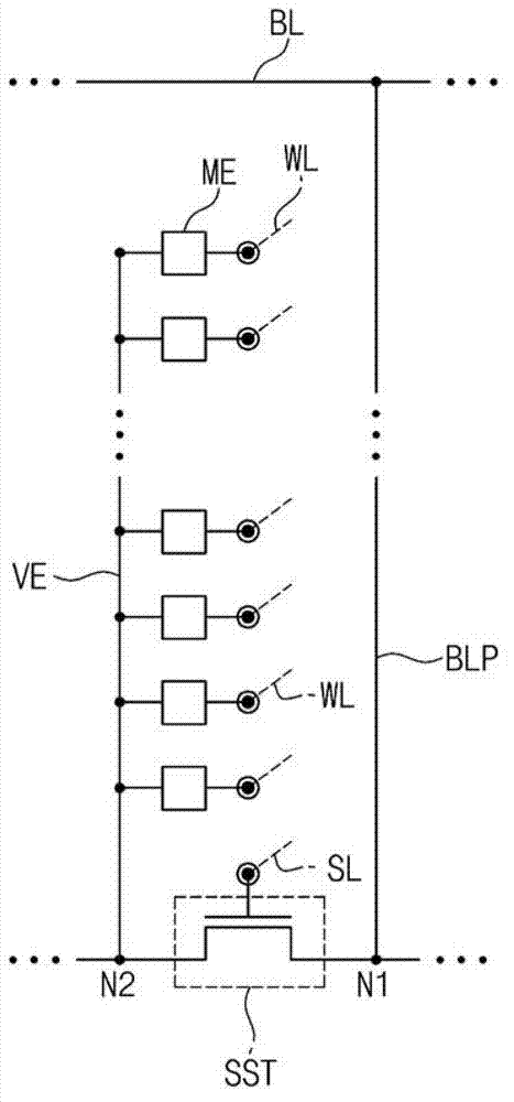
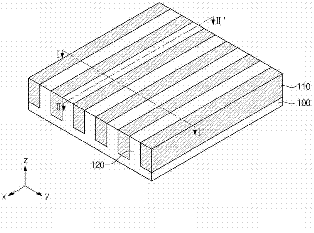
Semiconductor memory devices are provided. The device may include may include first and second selection lines connected to each other to constitute a selection line group, a plurality of word lines sequentially stacked on each of the first and second selection lines, vertical electrodes arranged in a row between the first and second selection lines, a plurality of bit line plugs arranged in a row at each of both sides of the selection line group, and bit lines crossing the word lines and connecting the bit line plugs with each other.

Description

[0001] Cross References to Related Applications [0002] This application claims priority from Korean Patent Application No. 10-2011-0124204 filed on Nov. 25, 2011, the entire contents of which are incorporated herein by reference. technical field [0003] Example embodiments of inventive concepts relate to semiconductor memory devices, and more particularly, to semiconductor memory devices having three-dimensionally arranged resistive memory cells. Background technique [0004] Three-dimensional integrated circuit (3D-IC) memory technology can be used to increase memory capacity. The 3D-IC memory technology generally refers to a technology related to three-dimensionally arranging memory cells. In addition to 3D-IC memory technology, memory capacity can also be increased by (1) pattern miniaturization technology and (2) multi-level cell (MLC) technology. However, the use of pattern miniaturization techniques can be limited due to high cost, and the increase in capacity ach...

Claims


Application Information

Patent Timeline
Patent Type & Authority Applications(China)
IPC IPC(8): H01L27/24H01L45/00H10N89/00H10N80/00H10N99/00
CPCH01L45/147H01L45/144H01L27/249H01L27/2436H01L45/06H01L45/148H01L27/24H01L45/00H01L45/143H01L45/141H01L45/146H01L45/145H01L45/1226H01L27/228H01L45/04H10B63/845H10B63/30H10B61/22H10N70/823H10N70/231H10N70/20H10N70/884H10N70/8836H10N70/8828H10N70/8833H01L27/0688H10N70/882
Inventor 朴镇泽朴泳雨崔正达
Owner SAMSUNG ELECTRONICS CO LTD
Why Eureka
Eureka Blog
Learn More