
Naked eye three-dimensional (3D) grating structure

A grating structure, 3D technology, applied in the direction of optics, optical components, instruments, etc., can solve the problem that it is difficult to see the 3D effect, and achieve the effect of ensuring the 3D effect

Inactive Publication Date: 2013-06-19
WUHAN TIANMA MICRO ELECTRONICS CO LTD
View PDF10 Cites 12 Cited by
  • Summary
  • Abstract
  • Description
  • Claims
  • Application Information

AI Technical Summary

Problems solved by technology

At present, the grating uses the shielding area made of electrodes. When the electrodes are energized, the upper and lower electric fields are formed to flip the liquid crystal to form a shield. However, in the existing 3D grating structure under the naked-eye 3D technology, the electrode line width and the width of the gap are different. It is fixed. Once there is an offset between the grating and the TFT module, it is difficult to see the 3D effect. At the same time, it is difficult to separate the two after the grating and the TFT are bonded again.

Method used


Image

  • Naked eye three-dimensional (3D) grating structure
  • Naked eye three-dimensional (3D) grating structure
  • Naked eye three-dimensional (3D) grating structure

Examples


Embodiment 1

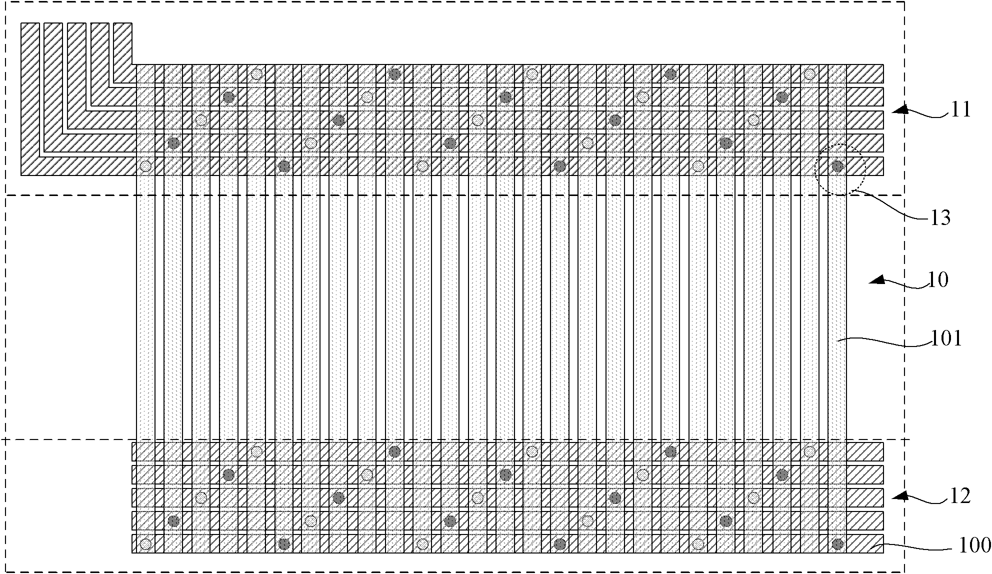
[0022] Such as figure 1 As shown, this embodiment provides a naked-eye 3D grating structure, including a grating region 10 and shorting bar regions 11, 12 electrically connected thereto, wherein the grating region 10 has grating bars 101 uniformly distributed at equal intervals; The bar areas 11 and 12 are located at the edge of the grating area 10 and include a plurality of shorting bars 100 , and each shorting bar 100 is connected with a plurality of grating bars 101 .

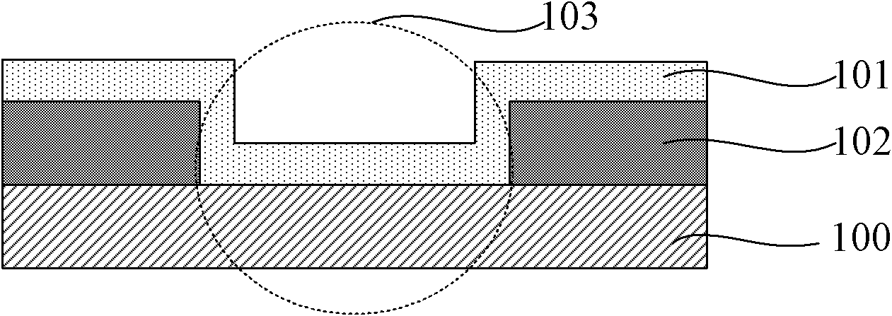
[0023] In this example, if figure 2 As shown, in the structure of the junction 13 between the shorting bar areas 11, 12 and the grating strips, the shorting bar 101 is a metal layer, which is used as a peripheral circuit; There is also a layer of insulating medium 102 between 101 and the overlapping area of ​​the shorting bar 100 .

[0024] In this embodiment, in the shorting bar area, every fourth grating bar is connected to the same shorting bar, and each shorting bar can be individually controlled to b...

Embodiment 2

[0029] Such as Figure 5 As shown, this embodiment provides a naked-eye 3D grating structure, which is a two-dimensional structure, including a grating region 30 and shorting bar regions 31 , 32 , 33 , 34 electrically connected thereto. Wherein, the grating area 30 includes grating strips 301 uniformly distributed at equal intervals in the horizontal direction and grating strips 302 evenly distributed at equal intervals in the vertical direction; Shorting bars, used to connect and control the grating strips 301 that are equally spaced and evenly distributed in the vertical direction; the shorting areas 32, 34 are located on the edges of the grating area 30 in the horizontal direction, and contain several shorting bars 300, used to connect and control the horizontal The grating strips 301 are uniformly distributed at equal intervals in the direction. In this embodiment, the shorting bar areas 31 , 32 , 33 , and 34 are connected to the same shorting bar every four grating bars,...


PUM


Abstract

The invention provides a naked eye three-dimensional (3D) grating structure. According to the fact that a plurality of short circuit bars are respectively connected with grating strips and individually control the grating strips, after a grating is attached to a thin film transistor (TFT), the line width and the position of a line seam of the grating can be changed so that assembling off-position is matched, and a 3D effect is ensured.

Description

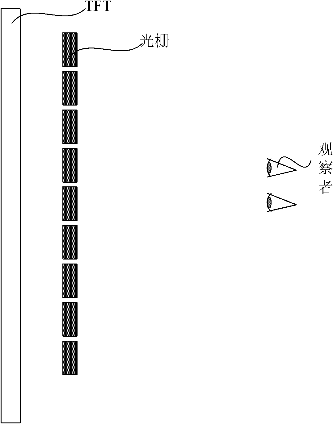
technical field [0001] The invention relates to the technical field of stereoscopic display, in particular to a naked-eye 3D grating structure. Background technique [0002] With the rise of 3D, naked-eye 3D has also attracted much attention. At present, there are four main types of naked-eye 3D technologies: electronic visual barrier grating, lenticular lens technology, shutter interference backlight and double-layer display. Among them, the electronic visual barrier grating technology is also called parallax barrier or parallax barrier technology. Its principle is to use a separate grating and TFT bonding method to allow the observer's left and right eyes to see with a fixed line width and seam. to different screens to form a 3D effect. At present, the grating uses the shielding area made of electrodes. When the electrodes are energized, the upper and lower electric fields are formed to flip the liquid crystal to form a shield. However, in the existing 3D grating structur...

Claims


Application Information

Patent Timeline
Patent Type & Authority Applications(China)
IPC IPC(8): G02B27/22
Inventor 易文佳赵朝军郭华强兆芃
Owner WUHAN TIANMA MICRO ELECTRONICS CO LTD
Learn More