A method for manufacturing a capacitive screen sensor without etching marks

A production method and capacitive screen technology, applied in the direction of electrical digital data processing, input/output process of data processing, instruments, etc., can solve the problems of increasing cost, adding reflective layer, etc., to achieve water ripple elimination and avoid different effects

Inactive Publication Date: 2016-01-27
成都三利亚科技有限公司
View PDF5 Cites 0 Cited by
  • Summary
  • Abstract
  • Description
  • Claims
  • Application Information

AI Technical Summary

Problems solved by technology

In order to avoid the above problem 2, in the prior art, a layer of reflective layer is often specially made on the conductive film, and adding a reflective layer means increasing the cost

Method used


Image

  • A method for manufacturing a capacitive screen sensor without etching marks
  • A method for manufacturing a capacitive screen sensor without etching marks
  • A method for manufacturing a capacitive screen sensor without etching marks

Examples


Embodiment 1

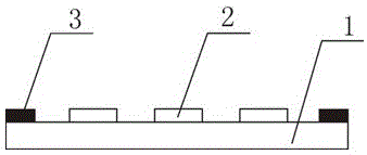
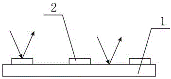
[0021] Embodiment 1: see Figure 1 to Figure 4 The thin film capacitor Sensor is composed of: a transparent substrate 1 is provided with a conductive layer 5, the conductive material around the conductive layer 5 is etched and provided with an electrode 3, the central conductive material of the conductive layer 5 is etched and provided with a pattern, and its Pattern area The schematic diagram of reflection and etching area etching reflection is as follows figure 2 shown.

[0022] The Sensor manufacturing process of the traditional thin-film structure is as follows:

[0023] Conductive film→baking shrinkage→conductive layer 5 is etched to form Pattern2→electrode 3 fabrication (involving baking).

[0024] In this manufacturing process, the etching of the conductive layer 5 at the electrode 3 is completed at the same time as the etching of the conductive layer 5 at the Pattern 2. However, after the electrode 3 is fabricated, a baking process will be involved, which will cause...


PUM


Abstract

The invention discloses a manufacture method of a capacitive screen Sensor without etching traces. The method comprises the following steps: (1), baking a conductive thin film for shrinking; (2), etching a conducting layer in the position of an electrode: etching off the conducting layer in an area of the conductive thin film, in which the electrode is arranged, through acid or etching cream; (3), arranging the electrode in the etched area; (4), placing the conductive thin film on which the electrode is arranged into a baking oven for baking; (5), etching a Pattern in the center of the conducting layer. The conventional capacitive screen Sensor manufacture method comprises the steps of manufacturing the conductive thin film, baking for shrinking, etching the conducting layer to form the Pattern, and manufacturing the electrode (referred to baking), while in the manufacture method provided by the invention, the step of manufacturing the electrode is advanced, and the step of etching the conducting layer to form the Pattern is postponed, the Pattern is not baked at high temperature after manufacture any more, which avoids the phenomenon that the deformation of a base material is different from that of the conducting layer, and further eliminates ripples.

Description

technical field [0001] The invention relates to a method for eliminating sensor etching marks, in particular to a method for manufacturing a capacitive screen sensor without etching marks. Background technique [0002] In recent years, touch panels have been widely used in various industries. Touch screen manufacturers have also sprung up like mushrooms. The competition among touch screen manufacturers is also becoming more and more fierce. As an important indicator for assessing the appearance of touch screens, how to eliminate etching marks has become an important topic. [0003] The thin film capacitor sensor of this touch screen is composed of: a conductive layer is provided on a transparent substrate, the conductive material around the conductive layer is etched and provided with electrodes, and the conductive material in the center of the conductive layer is etched and provided with elaborate patterns, that is, pattern. Etching marks refer to the difference between ...

Claims


Application Information

Patent Timeline
Patent Type & Authority Patents(China)
IPC IPC(8): G06F3/044
Inventor 唐桂昌
Owner 成都三利亚科技有限公司
Why Eureka
Try Eureka