A high breakdown voltage n-type vertical silicon carbide metal oxide semiconductor transistor

A semiconductor tube, silicon carbide technology, applied in semiconductor devices, circuits, electrical components, etc., can solve the problems of small breakdown voltage, strong electric field, device breakdown, etc., to achieve higher breakdown voltage, prevent local breakdown, improve The effect of breakdown voltage

A semiconductor tube, silicon carbide technology, applied in semiconductor devices, circuits, electrical components, etc., can solve the problems of small breakdown voltage, strong electric field, device breakdown, etc., to achieve higher breakdown voltage, prevent local breakdown, improve The effect of breakdown voltage

CN103400860BActive Publication Date: 2017-04-19SOUTHEAST UNIV

Image

  • A high breakdown voltage n-type vertical silicon carbide metal oxide semiconductor transistor
  • A high breakdown voltage n-type vertical silicon carbide metal oxide semiconductor transistor
  • A high breakdown voltage n-type vertical silicon carbide metal oxide semiconductor transistor

Examples


Embodiment Construction

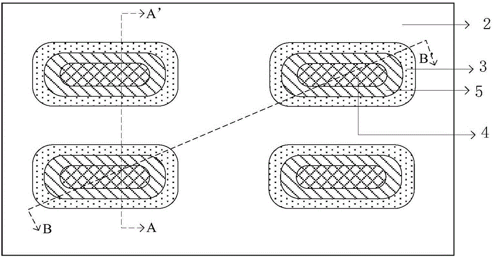
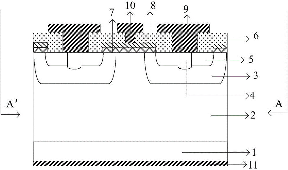
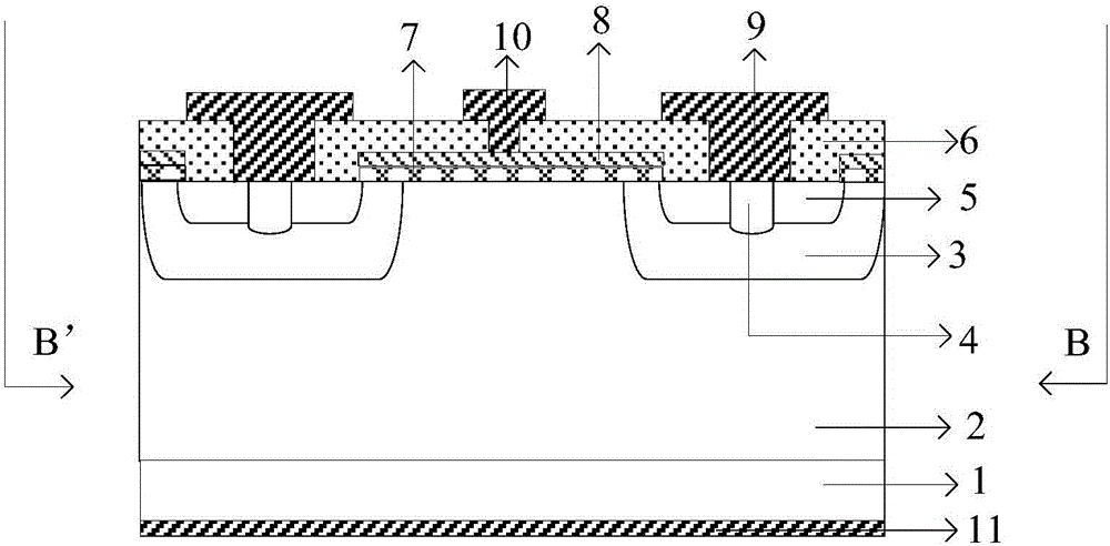
[0020] Combine below Figure 4 , Figure 5 and Figure 6 To describe the present invention in detail, a high breakdown voltage N-type vertical silicon carbide metal oxide semiconductor transistor includes: an N-type substrate 1, a drain metal 11 is connected to one side of the N-type substrate 1, and a drain metal 11 is connected to the N-type substrate 1. The other side of the type substrate 1 is provided with an N-type drift region 2, which is characterized in that a P-type base layer 3 is arranged on the N-type drift region 2, and a N-type base layer 3 distributed in an array is arranged on the P-type base layer 3. Type source region 5 and P type body contact region 4, be provided with N type drift region projection 12 formed by N type drift region 2 between every pair of adjacent N type source region 5, the boundary of N type drift region projection 12 Extending into the corresponding breakdown voltage enhancement region 13, the breakdown voltage enhancement region 13 is...


PUM


Abstract

An N type longitudinal silicon carbide MOS tube with high breakdown voltage comprises an N type substrate, wherein drain electrode metal and an N type drift region are arranged at two ends of the N type substrate respectively; a P type base region layer is arranged on the N type drift region; N type source regions and P type body contact regions distributed according to an array are arranged on the P type base region layer; N type drift region bulges are arranged between adjacent N type source regions; boundaries of the N type source regions extend into corresponding breakdown voltage improving regions; the breakdown voltage improving regions are rectangular regions formed by inner side boundary extension cords of four adjacent N type source regions; gate oxide layers are arranged on the N type drift region bulges, and boundaries of the gate oxide layers extend outwards and stop at the boundaries of the N type source regions; poly-silicon gates are arranged on the gate oxide layers; field oxide layers arranged on the poly-silicon gates and the N type source regions; the N type source regions and the P type body contact regions are connected with source electrode metal; and the surfaces of the poly-silicon gates are connected with gate metal.

Description

technical field [0001] The invention mainly relates to the field of high-voltage power semiconductor devices, specifically, an N-type vertical silicon carbide metal oxide semiconductor tube with high breakdown voltage, which is suitable for aerospace, aviation, oil exploration, nuclear energy and other fields. Background technique [0002] Silicon carbide material is a wide bandgap semiconductor material with large band gap, high breakdown voltage, high thermal conductivity, high electron saturation drift velocity, high electron mobility, high thermal conductivity, strong radiation resistance and chemical stability Excellent physical and chemical properties, such as good performance and compatibility with silicon integrated circuit technology, have become the preferred materials for manufacturing high-temperature, high-frequency, high-power, radiation-resistant, non-volatile memory devices and optoelectronic integrated devices. At present, developed countries represented by ...

Claims


Application Information

Patent Timeline
19 Apr 2017
Publication
CN103400860B
IPC
H01L29/78; H01L29/06
Inventors
孙伟锋; 黄宇