A Position Synchronization Method for Defect Detection and Observation Equipment

A defect detection and equipment technology, which is applied in semiconductor/solid-state device testing/measurement, material analysis by measuring secondary emissions, electrical components, etc., can solve problems such as lack of effective synchronization methods, and achieve the goal of avoiding the failure of automatic observation Effect

Active Publication Date: 2017-07-07
SHANGHAI HUALI MICROELECTRONICS CORP
View PDF5 Cites 0 Cited by
  • Summary
  • Abstract
  • Description
  • Claims
  • Application Information

AI Technical Summary

Problems solved by technology

But the patent still lacks effective synchronization method

Method used


Image

  • A Position Synchronization Method for Defect Detection and Observation Equipment
  • A Position Synchronization Method for Defect Detection and Observation Equipment
  • A Position Synchronization Method for Defect Detection and Observation Equipment

Examples


Embodiment Construction

[0026] The present invention will be further described below in conjunction with the accompanying drawings and specific embodiments. Obviously, the described examples are only some examples of the present invention, not all examples. Based on the examples summarized in the present invention, all examples obtained by persons of ordinary skill in the art without making creative efforts belong to the protection scope of the present invention.

[0027] It should be noted that, in the case of no conflict, the examples in the present invention and the features in the examples can be freely combined with each other.

[0028] An example of the present invention will be explained in detail below in conjunction with the accompanying drawings.

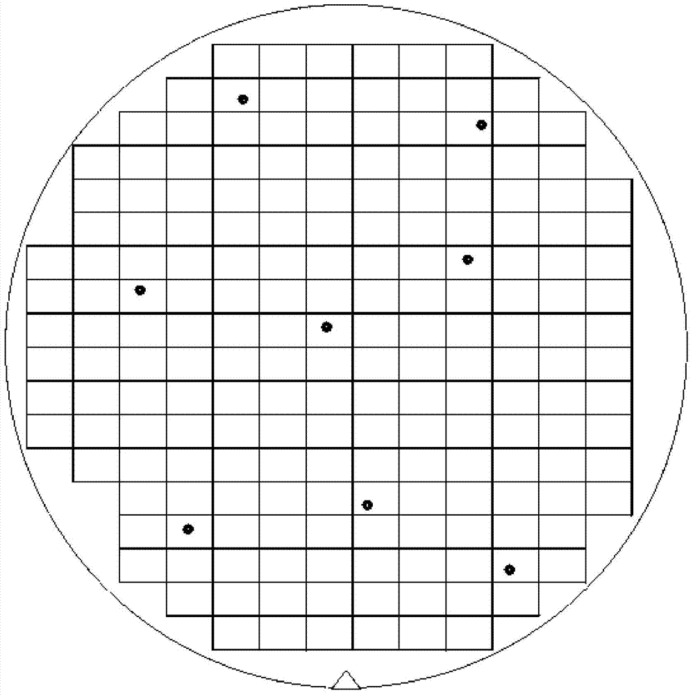
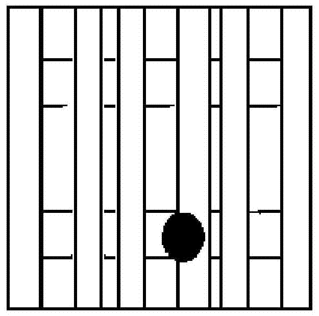
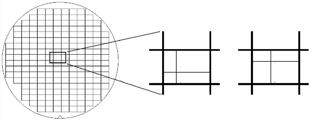
[0029] The example of the present invention is applied to the detection and observation of wafer defects, and the defect detection and observation equipment includes defect detection equipment and defect observation equipment, wherein the method ...


PUM


Abstract

The invention provides a position synchronizing method of defect detection and observation devices, relating to the technical field of semiconductor detection. The method comprises the steps that a reference wafer with a defect is provided; the defect detection device detects the reference wafer, and the defect observation device observes the defect, and corrects a defect observation program according to a first deviation value; after a set time interval, the defect detection and observation devices respectively detects and observes the defect of the reference wafer again to obtain a second deviation value of the central positions of the defect detection and observation devices; and the first deviation value is corrected and updated according to the second deviation value. According to technical scheme of the invention, the central positions of the defect detection and observation devices are kept consistent, thereby avoiding failure of automatic observation due to great difference between the defect detection and observation devices.

Description

technical field [0001] The invention relates to the field of semiconductor detection technology, in particular to a method for position synchronization of defect detection and observation equipment. Background technique [0002] The manufacturing process of integrated circuits is very complicated. Simply put, it is to use various methods to form different "layers" on the substrate material (such as silicon substrate), and to dope ions in selected areas to change the semiconductor material. Conductive properties, the process of forming semiconductor devices. The manufacturing process of integrated circuits is composed of a variety of individual processes. Simply put, the main individual processes usually include three categories: thin film preparation process, pattern transfer process and doping process. [0003] In order to meet the computing requirements of the complex functions of the chip, the critical dimensions of the circuit graphics on the chip are continuously reduc...

Claims


Application Information

Patent Timeline
Patent Type & Authority Patents(China)
IPC IPC(8): H01L21/66H01L21/68G01N23/22
CPCH01L22/12H01L22/20
Inventor 倪棋梁陈宏璘龙吟
Owner SHANGHAI HUALI MICROELECTRONICS CORP
Why Eureka
Try Eureka