Suction cup and method for eliminating wafer exposure out-of-focus defects

A technology of wafers and chucks, which is applied in the direction of electrical components, semiconductor/solid-state device manufacturing, circuits, etc., can solve problems such as wafer breakage and lower product yield, and achieve the elimination of warping and deformation positions, elimination of out-of-focus defects, and improvement of Effect of Exposure Quality and Product Yield

Active Publication Date: 2017-07-25
SHANGHAI HUALI MICROELECTRONICS CORP
View PDF4 Cites 0 Cited by
  • Summary
  • Abstract
  • Description
  • Claims
  • Application Information

AI Technical Summary

Problems solved by technology

Patent Publication No. CN 103367217A discloses a silicon wafer adsorption device and its adsorption method. Although the suction cup has vacuum suction holes to adsorb the wafer, the wafer does not have warping deformation or warping deformation is small In some cases, it can meet the requirements of fixing the wafer and improving the warpage of the wafer. However, in the case of serious warpage, simply relying on increasing the vacuum degree to increase the mechanical force applied to the wafer will be due to the force If it is too large, it will lead to the breakage of the wafer and reduce the product yield; under the condition of increasing the vacuum degree, it is impossible to completely eliminate the defect of wafer warping and deformation, so the defect of exposure out-of-focus will still exist

Method used


Image

  • Suction cup and method for eliminating wafer exposure out-of-focus defects
  • Suction cup and method for eliminating wafer exposure out-of-focus defects
  • Suction cup and method for eliminating wafer exposure out-of-focus defects

Examples


Embodiment Construction

[0030] In order to make the content of the present invention clearer and easier to understand, the content of the present invention will be further described below in conjunction with the accompanying drawings. Of course, the present invention is not limited to this specific embodiment, and general replacements known to those skilled in the art are also covered within the protection scope of the present invention.

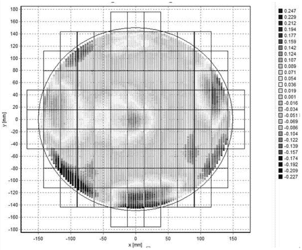
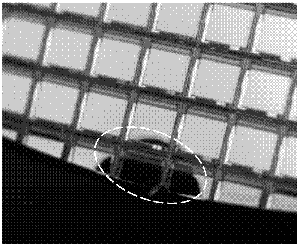
[0031] As mentioned above, due to the warpage and deformation of the wafer, it will cause out-of-focus defects during the exposure process, and the existing method simply increases the force acting on the wafer by increasing the vacuum degree of the vacuum suction hole. To reduce its deformation, because the force applied to the wafer cannot be increased without limit, so, in the case of severe wafer warpage, simply increasing the vacuum degree of the vacuum suction hole still cannot eliminate the deformation of the wafer. Warpage defects, and thus out-of-focus def...


PUM


Abstract

The invention provides a sucker and method for eliminating wafer exposure defocus defects. The sucker is flat in upper surface and is used for supporting a wafer. The sucker comprises a plurality of vacuum suction holes and a plurality of thermoelectric couples, the vacuum suction holes are densely distributed in the upper surface of the sucker, all parts of the wafer are absorbed into the same plane by the vacuum suction holes, the thermoelectric couples are densely distributed at the bottom of the sucker, the thermoelectric couples and the vacuum suction holes are alternatively arranged, and the thermoelectric couples are used for heating the wafer. By means of the sucker and method, the thermoelectric couples densely distributed at the bottom of the sucker and the vacuum suction holes densely distributed in the upper surface of the sucker are arranged, the upper surface of the sucker is flat, stress in the wafer is slowly released in the heating process, vacuum suction force, acting on the wafer, of the vacuum suction holes enables the wafer to be attached to the flat upper surface of the sucker, buckling deformation defects of the wafer are accordingly reduced, the surface of the wafer is flattened, the defocus defects in the exposure process are further eliminated, and the exposure quality and the product yield are improved.

Description

technical field [0001] The invention relates to the technical field of semiconductors, in particular to a chuck for eliminating out-of-focus defects in wafer exposure and a method for eliminating out-of-focus defects in wafer exposure. Background technique [0002] In the semiconductor manufacturing process, after going through multiple processes, a large amount of stress will inevitably accumulate on the wafer, causing the wafer to warp and deform. Such as figure 1 Shown is a schematic diagram of the test height difference of the wafer, figure 1 In , darker colors indicate upward or downward warping, and larger numbers indicate greater deformation. Wafer warpage will affect the quality of the exposure process. Specifically, the exposure equipment cannot fully compensate for the focal depth of focus, making the exposure out of focus, such as figure 2 as shown, figure 2 is a schematic diagram of the exposure of the wafer with out-of-focus defects, figure 2 In , black...

Claims


Application Information

Patent Timeline
Patent Type & Authority Patents(China)
IPC IPC(8): H01L21/683
CPCH01L21/67103H01L21/6838
Inventor 王剑
Owner SHANGHAI HUALI MICROELECTRONICS CORP
Why Eureka
Try Eureka