Analog accumulator applied to TDI (time delay integral)-type CMOS (complementary metal-oxide-semiconductor transistor) image sensor

An image sensor and accumulator technology, applied in image communication, color TV parts, TV system parts, etc., can solve the problems of reducing the integral effect, reducing the accumulation effect, etc., and achieve simple structure and increase the effective accumulation series Effect

Active Publication Date: 2015-04-08
TIANJIN UNIV
View PDF4 Cites 6 Cited by
  • Summary
  • Abstract
  • Description
  • Claims
  • Application Information

AI Technical Summary

Problems solved by technology

For the impact of parasitic, it can be intuitively understood that during each integration, the parasitic capacitance is mounted on the input and output terminals of the op amp, forming negative feedback, reducing the integration effect, thereby reducing the accumulation effect, and inhibiting the effective accumulation series. promote

Method used


Image

  • Analog accumulator applied to TDI (time delay integral)-type CMOS (complementary metal-oxide-semiconductor transistor) image sensor
  • Analog accumulator applied to TDI (time delay integral)-type CMOS (complementary metal-oxide-semiconductor transistor) image sensor
  • Analog accumulator applied to TDI (time delay integral)-type CMOS (complementary metal-oxide-semiconductor transistor) image sensor

Examples


Embodiment Construction

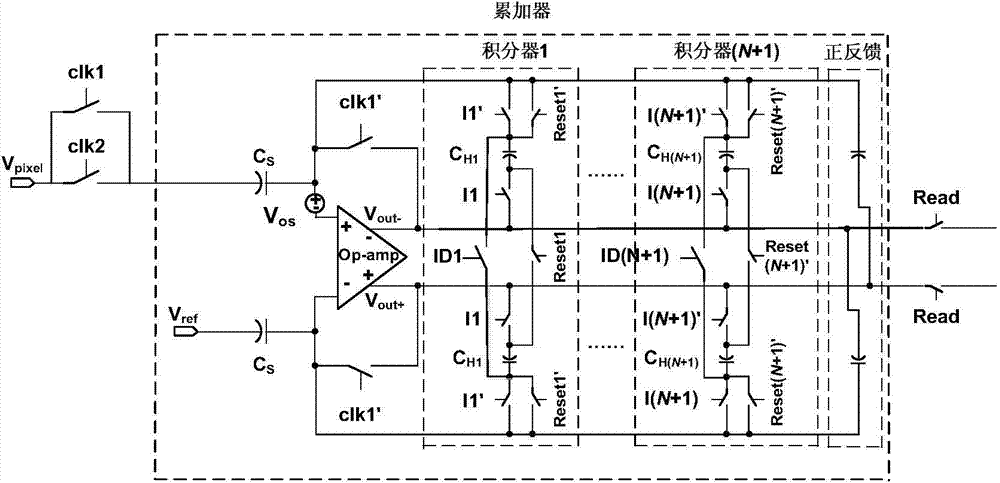
[0013] The invention improves the analog accumulator used in the TDI CIS, and realizes the compensation for the influence caused by the parasitic by adding a positive feedback capacitor. It can greatly increase the number of effective accumulation stages of the accumulator without excessively increasing the area and power consumption of the circuit.

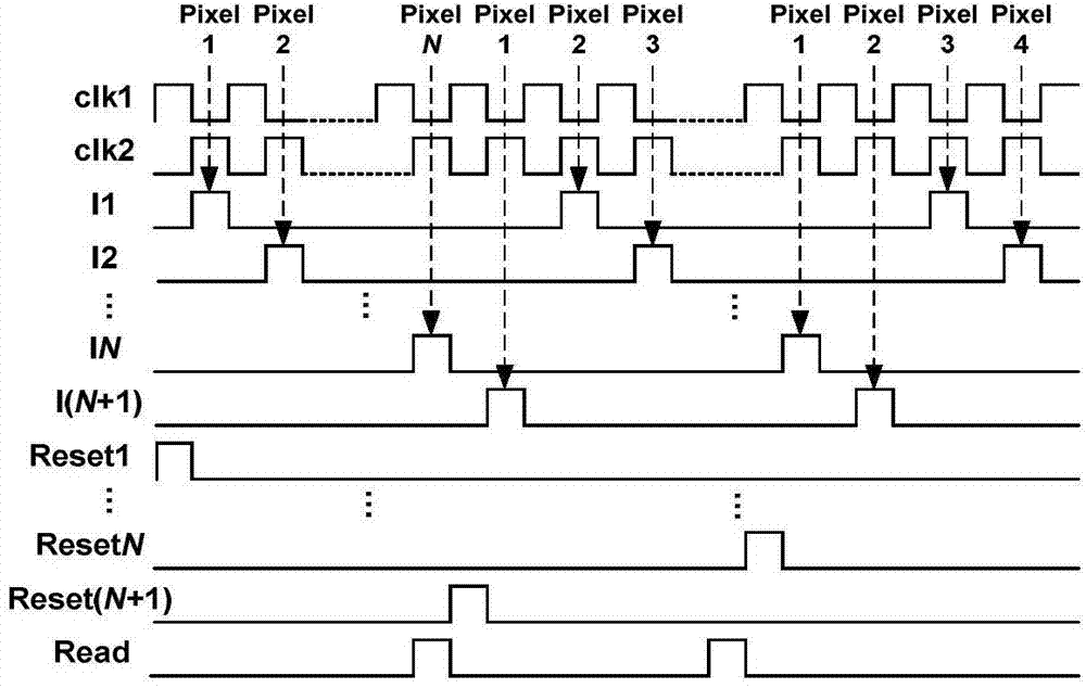
[0014] figure 1 The structural diagram of the analog accumulator proposed by the present invention includes an operational amplifier, an N+1-level integrator, a sampling switch, an integrating switch and a positive feedback capacitor, and N-level pixel signal accumulation can be realized through time oversampling technology. The operational amplifier is implemented with a fully differential structure, and the sampling capacitor is connected to the input terminal of the sampling switch clk1, the integrating switch clk2 and the operational amplifier, and clk1 is connected to the pixel signal or bias voltage at the same time. Anoth...


PUM


Abstract

The invention relates to the field of integrated circuit design; in order to realize the compensation of the influence brought to parasitism, the effective accumulation series of the accumulator is greatly increased, and meanwhile, the area and the power consumption of a circuit are not increased excessively. Therefore, the technical scheme adopted by the invention is that an analog accumulator applied to a TDI (time delay integral)-type CMOS (complementary metal-oxide-semiconductor transistor) image sensor comprises an operational amplifier, an N+1-stage integrator, a sampling switch and an integral restrictor, and also comprises two positive feedback capacitors; one of the two positive feedback capacitors is connected between the positive input end and the positive output end of the operational amplifier, and the other positive feedback capacitor is connected between the negative input end and the negative output end of the positive feedback capacitor. The analog accumulator disclosed by the invention is mainly applied to the integrated circuit design.

Description

technical field [0001] The invention relates to the field of integrated circuit design, in particular to a device and method for compensating the parasitic implementation of an analog accumulator in a CMOS type TDI image sensor. Specifically, it relates to an analog accumulator applied to a TDI-type CMOS image sensor technical background [0002] Time delay integration (TDI) image sensor is a special kind of single row image sensor. Compared with ordinary single-line image sensors, TDI image sensors accumulate N times of pixel signals through multiple acquisitions of the same object. Since the signal increases by N times during the accumulation process, the noise increases during the accumulation process. times, so the output image signal-to-noise ratio (SNR) is improved times. Therefore, the TDI image sensor can obtain low-noise output images at high moving speeds and low light intensity. [0003] Early TDI image sensors were mainly realized by CCD image sensors, beca...

Claims


Application Information

Patent Timeline
Patent Type & Authority Applications(China)
IPC IPC(8): H04N5/3745H04N5/353
Inventor 徐江涛黄福军聂凯明高志远史再峰高静姚素英
Owner TIANJIN UNIV
Why Eureka
Try Eureka