Image sensor parasitism insensitiveness simulation accumulator and time sequence control method

An image sensor and accumulator technology, which is applied in image communication, TV, color TV components and other directions, can solve problems such as reducing the accumulation effect, and achieve the effect of no increase in power consumption, a simple structure, and an increase in the number of effective accumulation stages.

Inactive Publication Date: 2015-04-15
TIANJIN UNIV
View PDF4 Cites 1 Cited by
  • Summary
  • Abstract
  • Description
  • Claims
  • Application Information

AI Technical Summary

Problems solved by technology

In fact, due to the influence of the internal parasitics of the integrator, the charge in the sampling capacitor cannot be completely transferred to the integrating capacitor, but will be partially absorbed by the equivalent parasitic capacitance of the idle integrator, thereby reducing the accumulation effect

Method used


Image

  • Image sensor parasitism insensitiveness simulation accumulator and time sequence control method
  • Image sensor parasitism insensitiveness simulation accumulator and time sequence control method
  • Image sensor parasitism insensitiveness simulation accumulator and time sequence control method

Examples


Embodiment Construction

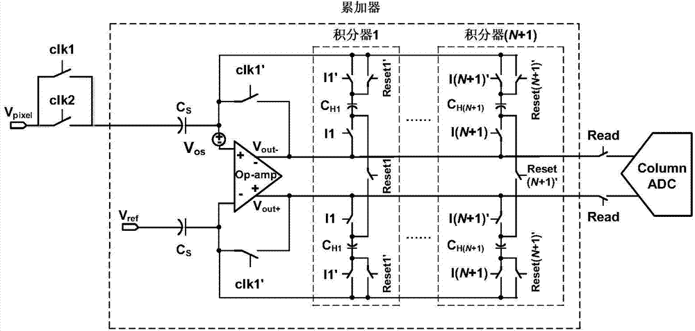
[0020] The invention improves the analog accumulator used in the TDI CIS, and reduces the limitation of parasitic in the circuit to the number of accumulation stages by adding a decoupling switch. It can greatly increase the number of effective accumulation stages of the accumulator without increasing the area and power consumption of the circuit.

[0021] The technical scheme adopted in the present invention is:

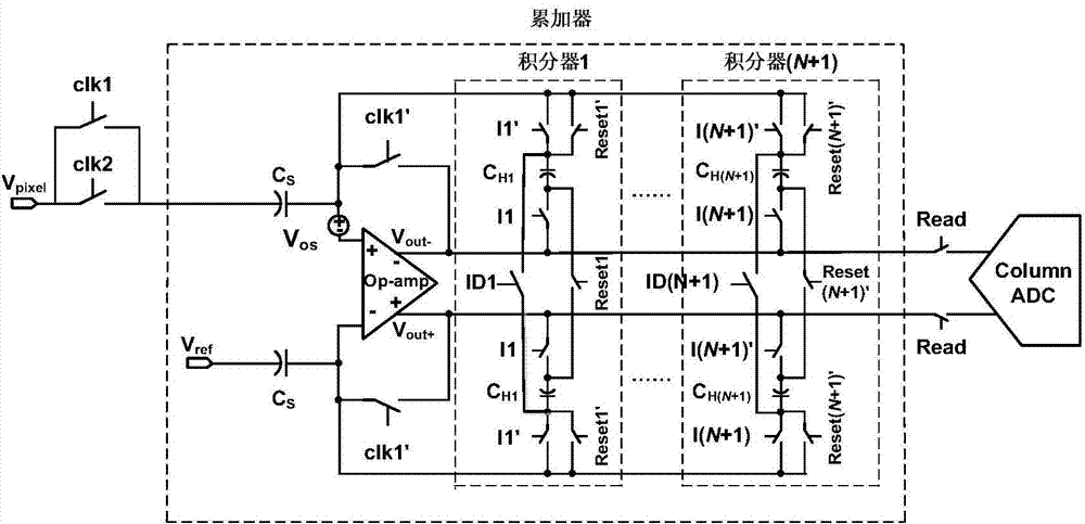
[0022] image 3 It is the structural diagram of the analog accumulator proposed by the present invention. In order to realize the elimination of parasitic, it adds a decoupling switch ID in each stage integrator on the basis of the existing accumulator, and connects the two integration capacitors Upper plate. The structure eliminates the parasitic in the integrator by controlling the decoupling switch, and greatly increases the effective accumulation stages of the accumulator.

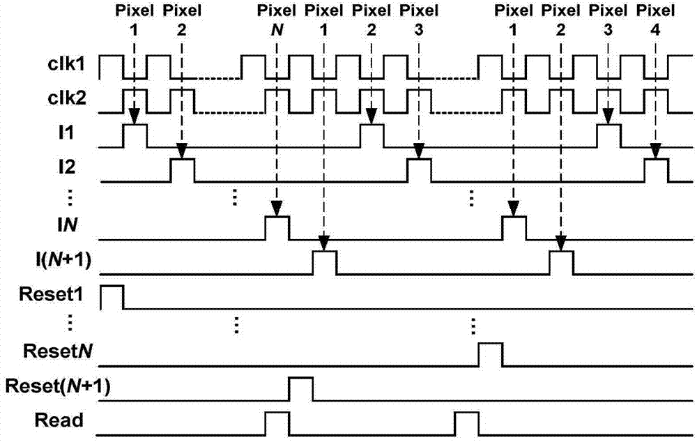
[0023] Figure 4 It is the timing diagram of the analog accumulator proposed by the ...


PUM


Abstract

The invention relates to the field of integrated circuit design. In order to improve a simulation accumulator applied to a TDI CIS, greatly increase effective accumulative levels of the accumulator, and not increase the area and the power consumption of a circuit, the invention adopts the technical scheme as follows: the image sensor parasitic insensitiveness simulation accumulator comprises an operational amplifier, N+1 levels of integrators, a sampling switch and integrating switches, each level of integrator consists of four integrating switches, two integrating capacitors and two reset switches; a decoupling switch is arranged in each level of integrator; the decoupling switch is connected between upper electrode plates of the two integrating capacitors. The technical scheme provided by the invention is mainly applied to the integrated circuit design.

Description

technical field [0001] The invention relates to the field of integrated circuit design, in particular to a realization method for eliminating the parasitic of an analog accumulator in a CMOS type TDI image sensor. Specifically, it relates to an image sensor parasitic insensitive analog accumulator and a timing control method. technical background [0002] Time delay integration (TDI) image sensor is a special kind of single row image sensor. Compared with ordinary single-line image sensors, TDI image sensors accumulate N times of pixel signals through multiple acquisitions of the same object. Since the signal increases by N times during the accumulation process, the noise increases during the accumulation process. times, so the output image signal-to-noise ratio (SNR) is improved times. Therefore, the TDI image sensor can obtain low-noise output images at high moving speeds and low light intensity. [0003] Early TDI image sensors were mainly realized by CCD image sens...

Claims


Application Information

Patent Timeline
Patent Type & Authority Applications(China)
IPC IPC(8): H04N5/3745H04N5/353
Inventor 徐江涛黄福军聂凯明史再峰高静高志远姚素英
Owner TIANJIN UNIV
Why Eureka
Try Eureka