

Laser direct writing method based on large-area multi-step binary optical element
A binary optical element, laser direct writing technology, applied in microlithography exposure equipment, diffraction grating, photolithography process exposure device and other directions, can solve the problem of high precision, large area, multi-step binary optical exposure efficiency has no advantages problems, to achieve the effect of precise control of exposure metering, reduction of error probability, and improvement of lithography efficiency
- Summary
- Abstract
- Description
- Claims
- Application Information
AI Technical Summary
Problems solved by technology
Method used
Image

Examples
Embodiment Construction
[0038] The present invention will be described in detail below in conjunction with specific embodiments shown in the accompanying drawings. However, these embodiments do not limit the present invention, and any structural, method, or functional changes made by those skilled in the art according to these embodiments are included in the protection scope of the present invention.
[0039]The invention discloses a laser direct writing method based on a large-area multi-step binary optical element, including:
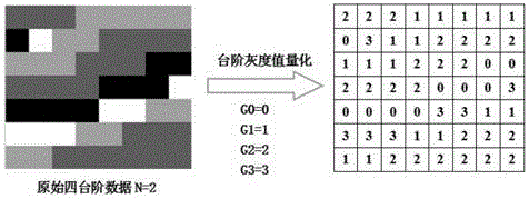
[0040] S1, will 2 N The sub-step data files are processed into gray values from G0=0 to G2 N -1=2 N A grayscale BMP image ending with -1, where 0 means no steps to be etched, 2 N -1 means the step with the deepest etching depth;
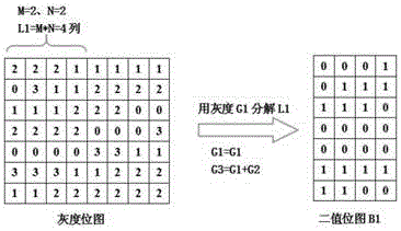
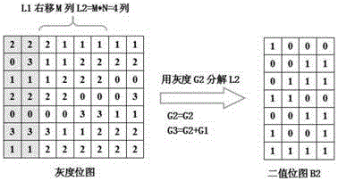
[0041] S2. According to the cumulative formula of exposure measurement P=P1+P2+...+Pn, Pn=2 n-1 *P1(nN Exposure metering required for sub-step exposure, and grayscale BMP images are divided into binary BMP bitmap queues B1 to Bm of several L...
PUM
 Abstract
Description
Claims
Application Information