Photoetching method of superfine structure

A lithography and structural material technology, applied in microlithography exposure equipment, optics, opto-mechanical equipment, etc., can solve the problems of low efficiency, difficulty in large-scale manufacturing, large amount of data, etc., to achieve simple process, solve manufacturing problems, low cost effect

Active Publication Date: 2013-07-03
INST OF MICROELECTRONICS CHINESE ACAD OF SCI
View PDF5 Cites 0 Cited by
  • Summary
  • Abstract
  • Description
  • Claims
  • Application Information

AI Technical Summary

Problems solved by technology

The electron beam lithography technology suitable for large-scale manufacturing of fine structures is usually a Gaussian scanning system with a resolution of several nanometers, but due to the need for fine line structures (such as gate structures with a width of Larger contact areas, source and drain areas, or layout routing areas) are scanned, and the main problem is low efficiency; the multi-beam electron beam exposure currently being developed has the problem of huge data volume, and it is difficult to be used on a large scale in the short term. manufacture

Method used


Image

  • Photoetching method of superfine structure
  • Photoetching method of superfine structure
  • Photoetching method of superfine structure

Examples


Embodiment Construction

[0028] The features and technical effects of the technical solution of the present invention will be described in detail below with reference to the accompanying drawings and in combination with exemplary embodiments. It should be pointed out that similar reference numerals represent similar structures, and the terms "first", "second", "upper", "lower", "thick", "thin" and the like used in this application can be used for Modify various device structures. These modifications do not imply a spatial, sequential or hierarchical relationship of the modified device structures unless specifically stated.

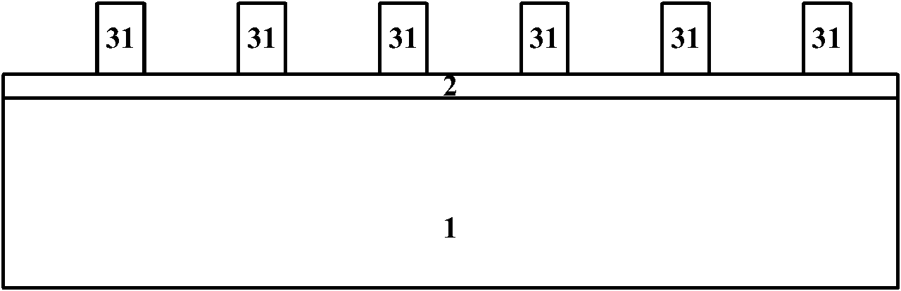
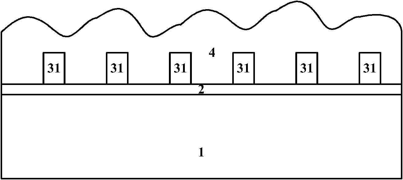
[0029] First, if figure 1 As shown, a structural material layer 2 and a first hard mask material layer 3 are sequentially formed on a substrate 1 . Wherein, the substrate 1 can be a common semiconductor material substrate such as bulk silicon, silicon-on-insulator (SOI), SiC, SiGe, sapphire, etc., and the substrate 1 can have shallow trench isolation STI to isolate and insulate ...


PUM


Abstract

The invention provides a photoetching method of a superfine structure. The photoetching method comprises the steps that: a structure material layer and a first hard mask material layer are formed on a substrate; a first photoetching is carried out for forming a first hard mask pattern; a second hard mask material layer is formed on the first hard mask pattern; and a second photoetching is carriedout for forming a second hard mask pattern, wherein light sources of the first photoetching and the second photoetching are different and are selected from either an i line mercury arc lamp or an electron beam exposure system. According to the photoetching method of the superfine structure provided by the invention, the traditional optical photoetching technology and the electronic beam photoetching technology are combined for use, the electronic beam exposure is used for realizing the superfine pattern manufacture, and the optical photoetching is used for completing other patterns, so the manufacture problem of the superfine pattern can be effectively solved, and the efficiency is not reduced.

Description

technical field [0001] The invention relates to the field of semiconductor device manufacturing, in particular to a microstructure hybrid photolithography method. Background technique [0002] With the development of very large scale integrated circuits for many years, the continuous reduction of circuit size has brought more and more challenges to process technology, especially photolithography technology. Based on efficiency considerations, the lithography technology currently used in mass production is mainly based on ultraviolet i-rays of different light source ranges (I-LINE, mercury arc lamps are used as light sources, and the emitted rays are i-lines with a wavelength of 365nm, which are in the ultraviolet band) And deep ultraviolet (DUV, usually using excimer laser as the light source, such as 248nm wavelength KrF excimer laser, 193nm ArF excimer laser) lithography technology, the immersion 193 lithography technology developed in recent years is the optical lithograp...

Claims


Application Information

Patent Timeline
Patent Type & Authority Patents(China)
IPC IPC(8): G03F7/00G03F1/20G03F7/20H01L21/027
Inventor 王红丽闫江
Owner INST OF MICROELECTRONICS CHINESE ACAD OF SCI
Why Eureka
Try Eureka