A kind of ferromagnetic semiconductor material (sr,na)(zn,mn)2as2 and preparation method thereof
A semiconductor, 2as2 technology, applied in the direction of material selection, inorganic material magnetism, etc., can solve the problem of low practical application value, and achieve the effect of enriching electrical transport properties and good stability
- Summary
- Abstract
- Description
- Claims
- Application Information
AI Technical Summary
Problems solved by technology
Method used
Image
Examples
Embodiment 1
[0058] This embodiment provides a method for preparing a ferromagnetic semiconductor material, including:
[0059] 1) Press (Sr 0.9 Na 0.1 )(Zn 0.95 mn 0.05 ) 2 As 2 The ratio of 2.3657 grams of Sr block, 3.7272 grams of Zn powder, 4.4203 grams of As powder, 0.1648 grams of Mn powder and 0.1439 grams of Na 3 Mix the As powder evenly, and put the mixture into an alumina ceramic test tube after being pressed into shape;
[0060] 2) Vacuum-encapsulate the ceramic test tube with the sample in the quartz tube and seal it;
[0061] 3) Put the quartz tube in a high temperature furnace for sintering at 670°C for 30 hours, and obtain a ferromagnetic semiconductor material (Sr 0.9 Na 0.1 )(Zn 0.95 mn 0.05 ) 2 As 2 .
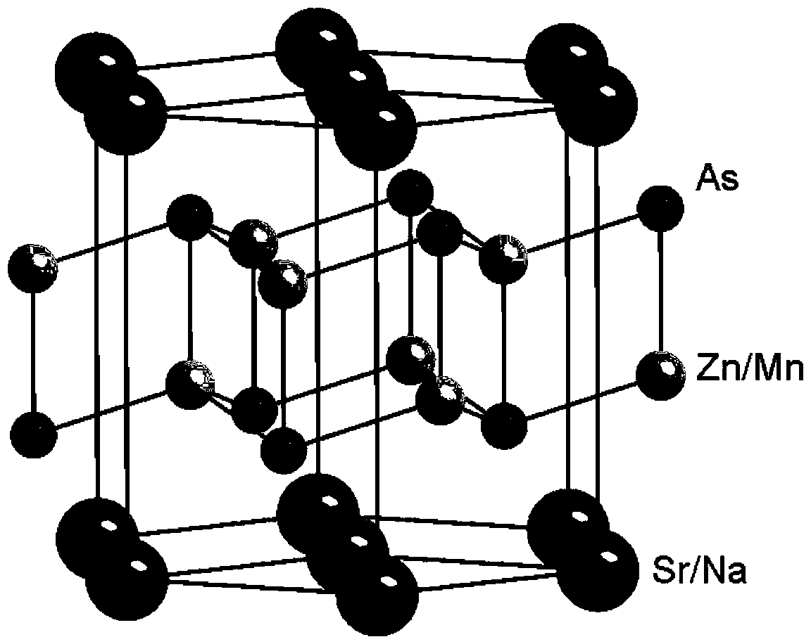
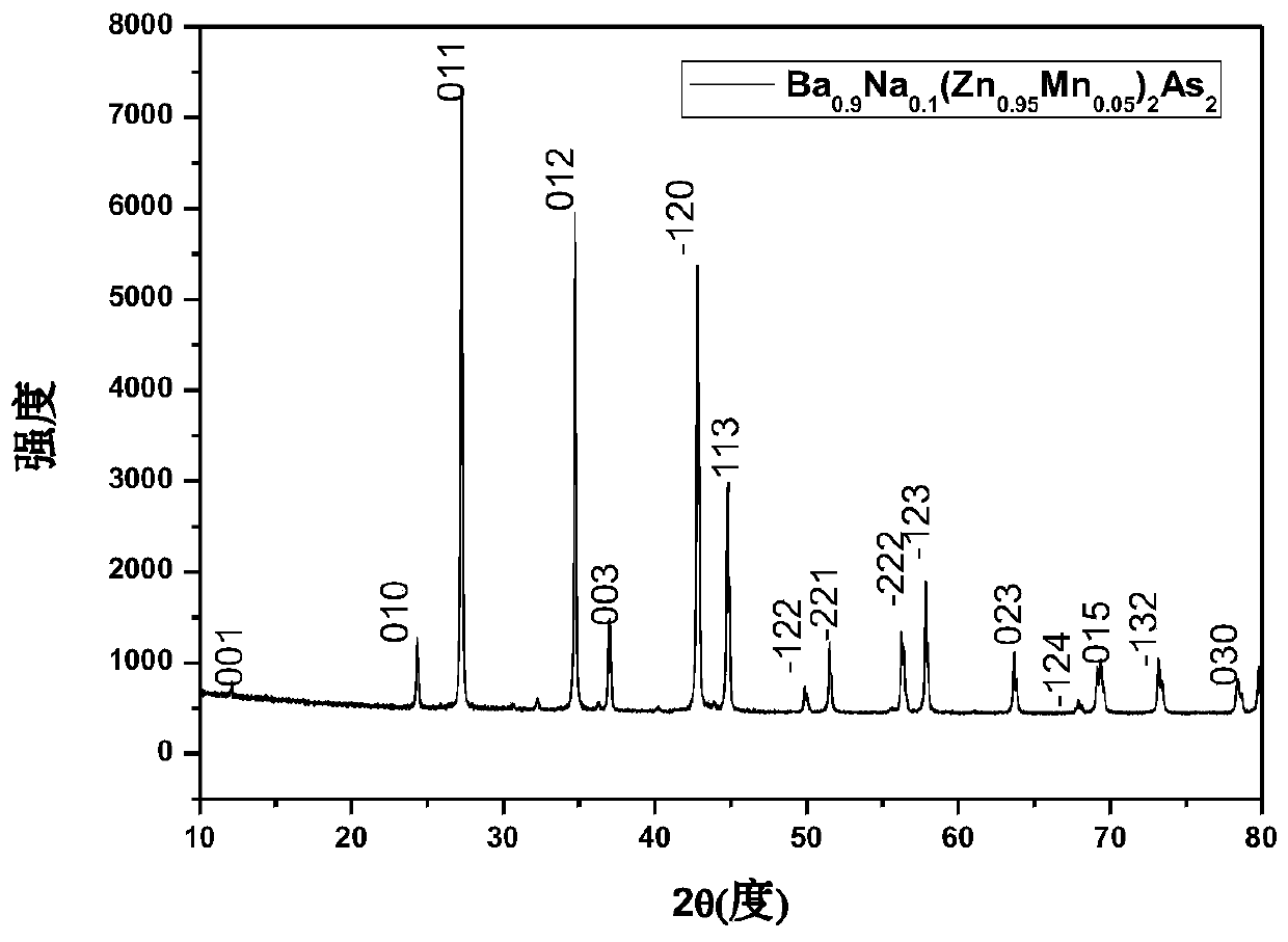
[0062] The X-ray diffraction pattern of the sample that the method of the present embodiment obtains is as figure 2 shown, from figure 2 It can be seen that the corresponding diffraction indices can be found for all the diffraction peaks of the sample, ind...
Embodiment 2
[0069] This embodiment provides a method for preparing a ferromagnetic semiconductor material, including:
[0070] 1) Press (Sr 0.9 Na 0.1 )(Zn 0.9 mn 0.1 ) 2 As 2 The ratio of 4.3885 grams of SrAs powder, 3.5311 grams of Zn powder, 2.3974 grams of As powder, 0.3296 grams of Mn powder and 0.1439 grams of Na 3 Mix the As powder evenly, and put the mixture into an alumina ceramic test tube;
[0071] 2) Vacuum seal the ceramic test tube with the sample in the quartz tube, fill the quartz tube with argon and seal it;
[0072] 3) The quartz tube is sintered at a temperature of 1000°C in a high-temperature furnace for 5 hours, and a ferromagnetic semiconductor material (Sr 0.9 Na 0.1 )(Zn 0.9 mn 0.1 ) 2 As 2 .
[0073] The X-ray diffraction pattern of the sample that the method of the present embodiment obtains is as Figure 7 shown, from Figure 7 It can be seen that the corresponding diffraction indices can be found for all the diffraction peaks of the sample, indic...
Embodiment 3
[0078] This embodiment provides a method for preparing a ferromagnetic semiconductor material, including:
[0079] 1) Press (Sr 0.9 Na 0.1 )(Zn 0.85 mn 0.15 ) ratio, 4.3885 grams of SrAs powder, 3.3349 grams of Zn powder, 2.3974 grams of As powder, 0.4945 grams of Mn powder and 0.1439 grams of Na 3 Mix the As powder evenly, put the mixture into the niobium tube, and seal the niobium tube under the protection of inert gas;
[0080] 2) Vacuum seal the niobium tube with the sample in the quartz tube, fill the quartz tube with argon and seal it;
[0081] 3) Sintering the quartz tube at a temperature of 700° C. in a high-temperature furnace for 20 hours;
[0082] 4) After the sintering is completed, the obtained sample is ground, mixed and pressed into tablets under the protection of argon gas, and put into a niobium tube, and the niobium tube is sealed under the protection of argon gas;
[0083] 5) Vacuum seal the niobium tube with the sample in the quartz tube, fill the qua...
PUM
| Property | Measurement | Unit |
|---|---|---|
| Curie point | aaaaa | aaaaa |
| Curie point | aaaaa | aaaaa |
| Curie point | aaaaa | aaaaa |
Abstract
Description
Claims
Application Information


