

Cadmium-based ferromagnetic semiconductor material and preparation method thereof
A semiconductor and ferromagnetic technology, which is used in the selection of materials, the magnetic properties of inorganic materials, and the manufacture of inductors/transformers/magnets. High transition temperature and good stability
- Summary
- Abstract
- Description
- Claims
- Application Information
AI Technical Summary
Problems solved by technology
Method used
Image

Examples
Embodiment 1
[0083] This embodiment provides a method for preparing a ferromagnetic semiconductor material, comprising the following steps:
[0084] 1) 3.153 grams of SrAs powder, 4.361 grams of Cd powder, 1.528 grams of As powder, 0.066 grams of Mn powder and 0.029 grams of Na 3 As powder is uniformly mixed (the atomic content ratio of Sr:Na:Cd:Mn:As is 0.97:0.03:1.94:0.06:2), and the mixture is pressed into an alumina ceramic test tube;
[0085] 2) Put the ceramic test tube with the reactant into the vacuum-sealed quartz tube;
[0086] 3) Put the quartz tube in a high-temperature furnace and sinter at a temperature of 700° C. for 30 hours.
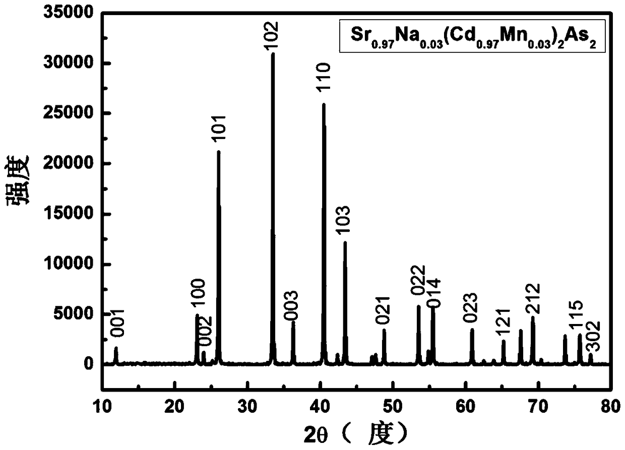
[0087] The block product obtained in step 3) was ground into powder, and subjected to X-ray diffraction analysis. figure 1 is its X-ray diffraction pattern, from figure 1 It can be concluded that the sample is a hexagonal crystal system, and all diffraction peaks have corresponding diffraction indices, and there are no miscellaneous peaks, that is...
Embodiment 2
[0094] This embodiment provides a method for preparing a ferromagnetic semiconductor material, comprising the following steps:
[0095] 1) 3.088 grams of SrAs powder, 4.272 grams of Cd powder, 1.548 grams of As powder, 0.11 grams of Mn powder and 0.048 grams of Na 3 As powder is evenly mixed (the atomic content ratio of Sr:Na:Cd:Mn:As is 0.95:0.05:1.90:0.10:2), and the mixture is put into a niobium tube under the protection of argon and sealed;
[0096] 2) Put the niobium tube containing the reactant into the quartz tube filled with argon and seal it;
[0097] 3) Put the quartz tube in a high-temperature furnace and sinter at a temperature of 750° C. for 20 hours;
[0098] 4) Grinding and mixing the sintered bulk material under the protection of argon, pressing it into tablets, putting it into a niobium tube and sealing it;
[0099] 5) Put the niobium tube into the quartz tube filled with argon and seal it;
[0100] 6) Put the quartz tube in a high-temperature furnace and s...
Embodiment 3
[0109] This embodiment provides a method for preparing a ferromagnetic semiconductor material, comprising the following steps:
[0110] 1) 3.007 grams of SrAs powder, 4.159 grams of Cd powder, 1.573 grams of As powder, 0.165 grams of Mn powder and 0.072 grams of Na 3 As powder is uniformly mixed (the atomic content ratio of Sr:Na:Cd:Mn:As is 0.925:0.075:1.85:0.15:2), and the mixture is put into a niobium tube under the protection of argon and sealed;
[0111] 2) Put the niobium tube containing the reactant into the quartz tube filled with argon and seal it;
[0112] 3) Put the quartz tube in a high-temperature furnace and sinter at a temperature of 800°C for 20 hours;
[0113] 4) Grinding and mixing the sintered bulk material under the protection of argon, pressing it into tablets, putting it into a niobium tube and sealing it;
[0114] 5) Put the niobium tube into the quartz tube filled with argon and seal it;
[0115] 6) Put the quartz tube in a high temperature furnace a...
PUM
| Property | Measurement | Unit |
|---|---|---|
| Curie point | aaaaa | aaaaa |
| Curie point | aaaaa | aaaaa |
| Curie point | aaaaa | aaaaa |
Abstract
Description
Claims
Application Information