
Organic light emitting compound, organic light emitting device comprising the same, and method of manufacturing the organic light emitting device

a light emitting device and organic technology, applied in the direction of organic chemistry, discharge tube luminescnet screen, anthracene dyes, etc., can solve the problems of poor and inferior material that can be used in solution coating in terms of thermal stability, color purity and the like, and achieve good solubility and high thermal stability

Inactive Publication Date: 2008-05-29
SAMSUNG ELECTRONICS CO LTD
View PDF8 Cites 161 Cited by
  • Summary
  • Abstract
  • Description
  • Claims
  • Application Information

AI Technical Summary

Benefits of technology

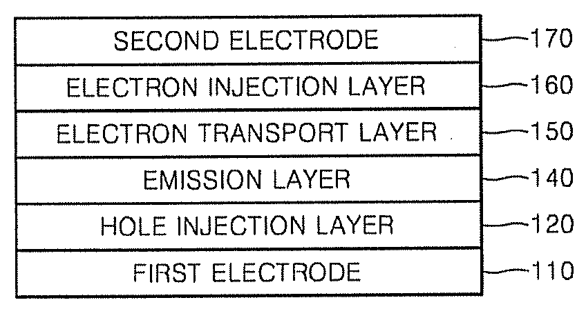
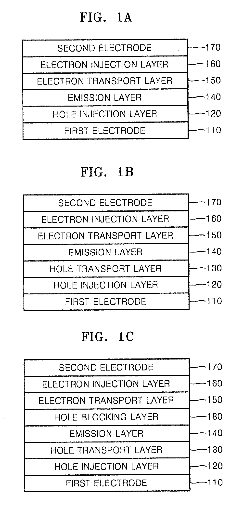
The patent text describes an organic light emitting compound that has good solubility and high thermal stability. The compound can be used in an organic light emitting device to improve its turn-on voltage, efficiency, color purity, and luminance. The compound has a specific formula and can be represented by a fused benzene ring or a fused naphthalene ring. The device includes a first electrode, a second electrode, and an organic layer between them, wherein the organic layer comprises the organic light emitting compound.

Problems solved by technology

When organic light emitting devices are manufactured using vacuum deposition, the manufacturing cost increases because of the use of a vacuum system.
In addition, when a shadow mask method is used for preparing pixels for natural color display, it is difficult to prepare high resolution pixels.
However, for OLED's that include blue light-emitting organic molecules, a material that can be used in solution coating is inferior to a material that can be used in vacuum deposition in terms of thermal stability, color purity and the like.
In addition, although such materials having good performance are used for preparing an organic layer, problems can arise where the material gradually crystallizes after the organic layer is prepared such that the size (largest dimension or length) of the crystal eventually formed approximates that of a wavelength of visible light.
As a result, visible light diffuses so that a whitening phenomenon can occur, and pin holes or the like can form, thereby causing degradation of the device.
However, the compound does not have sufficiently good solubility with respect to any useful solvent, and organic light emitting devices using such compounds therefore do not have satisfactory characteristics.

Method used


Image

  • Organic light emitting compound, organic light emitting device comprising the same, and method of manufacturing the organic light emitting device
  • Organic light emitting compound, organic light emitting device comprising the same, and method of manufacturing the organic light emitting device
  • Organic light emitting compound, organic light emitting device comprising the same, and method of manufacturing the organic light emitting device

Examples


synthesis example 1

[0095]Compound 3, represented by Formula 3, was synthesized according to Reaction Schemes 1, 2 and 3:

[0096]Synthesis of Intermediate A

[0097]8.4 g of 2,5-dibromonitrobenzene (30 mmol), 10.8 g of 1-naphthaleneboronic acid (62.6 mmol), 520 mg of tetrakis triphenylphosphine palladium (Pd(PPh3)4) (0.45 mmol) and 63 ml of a 2M aqueous potassium carbonate solution (126 mmol) were dissolved in 100 ml of toluene, respectively, and then the mixtures were added to a 500 ml round bottom flask under argon gas. Then, the mixture was refluxed for 24 hours. After the reaction was terminated, a solvent was removed by evaporation. Then, the residue washed with 500 ml of ethyl acetate and 500 ml of water. Thereafter, an organic layer was collected and dried over anhydrous magnesium sulfate. Subsequently, the dried organic layer was purified using silica chromatography to obtain 9.5 g of a compound represented by Intermediate A (yield 84%).

[0098]Synthesis of Intermediate B

[0099]8.0 g of Intermediate A ...

synthesis example 2

[0103]Compound 5 represented by Formula 5 was synthesized according to Reaction Schemes 4, 5 and 6:

[0104]Synthesis of Intermediate C

[0105]729 mg of 2-bromonitrobenzene (3.6 mmol), 1.1 g of 1-(4,4,5,5-tetramethyl-1,3,2-dioxaborolan-2-yl)anthracene (3.6 mmol), 63 mg of tetrakis triphenylphosphine palladium (Pd(PPh3)4) (0.054 mmol) and 3.8 ml of a 2M aqueous potassium carbonate (K2CO3) (7.6 mmol) were dissolved in 12 ml of toluene, respectively, and the mixtures were added to a 500 ml round bottom flask and then refluxed for 24 hours. After the reaction was terminated, the solvent was evaporated and thereby removed. Then, the residue washed with 100 ml of ethyl acetate and 100 ml of water. Thereafter, an organic layer was collected and dried with magnesium sulfate. Subsequently, the dried organic layer was purified using silica chromatography to obtain 880 mg of a compound represented by Intermediate C (yield 81%).

[0106]Synthesis of Intermediate D

[0107]806 mg of Intermediate C (2.7 mmo...

synthesis example 3

[0111]

[0112]Synthesis of Compound 14

[0113]840 mg of Intermediate D (3 mmol), 260 mg of copper (4.0 mmol), 1.2 g of potassium carbonate (8.4 mmol), 85 mg of 18-crown-6-ether (0.32 mmol), 540 mg of 2,3,4,5-tetraphenyl-4-bromophenyl (1 mmol) were dissolved in 6 ml of nitrobenzene, and the mixtures were added to a 500 ml round bottom flask and then refluxed for 24 hours. After the reaction was terminated, the solvent was evaporated and thereby removed. Then, the residue washed with 100 ml of ethyl acetate and 100 ml of water. Thereafter, an organic layer was collected and dried with magnesium sulfate. Subsequently, the dried organic layer was purified by silica chromatography to obtain 490 mg of a compound represented by Compound 14 (yield 67%).

[0114]1H-NMR (CDCl3, 300 MHz, ppm): 9.3-6.9 (m, 37H).


PUM

PropertyMeasurementUnit
temperatureaaaaaaaaaa
vapor pressureaaaaaaaaaa
Tmaaaaaaaaaa

Abstract

Provided are an organic light emitting compound represented by Formula 1 below, an organic light emitting device comprising the same, and a method of manufacturing the organic light emitting device:where CY1 and CY2 are each independently a fused C6-C50 aromatic ring, Ar1 is a substituted or unsubstituted C6-C50 arylene group, Ar2, Ar3, Ar4, and Ar5 are each independently a substituted or unsubstituted C6-C50 aryl group, m and n are independently 0-3, and R1 and R2 are substituent groups. An organic light emitting device comprising the organic light emitting compound has low turn-on voltage, high efficiency, high color purity and high luminance.

Description

[0001]This application claims priority to Korean Patent Application No. 10-2006-0117250, filed on Nov. 24, 2006, and all the benefits accruing therefrom under 35 U.S.C. §119(a), the disclosure of which is incorporated herein by reference in its entirety.BACKGROUND OF THE INVENTION[0002]1. Field of the Invention[0003]The present invention relates to an organic light emitting compound, an organic light emitting device comprising the same, and a method of manufacturing the organic light emitting device, and more particularly, to an organic light emitting compound that provides good electrical properties, high thermal stability and high photochemical stability, and that provides low turn-on voltage, high color purity and high luminance when the organic light emitting compound is used in an organic light emitting device, an organic light emitting device comprising the same, and a method of manufacturing the organic light emitting device.[0004]2. Description of the Related Art[0005]Light ...

Claims


Application Information

Patent Timeline
Patent Type & Authority Applications(United States)
IPC IPC(8): B05D5/12C07D209/56C07D209/80C07D487/22H01L51/50
CPCC07D209/80C09K11/06C09K2211/1007H05B33/14C09K2211/1014H01L51/0061H01L51/5012C09K2211/1011H10K85/636H10K50/11
Inventor SHIN, DONG-WOOHAN, EUN-SILPAEK, WOON-JUNGLYU, YI-YEOLKWON, O-HYUNKIM, MYEONG-SUKCHOI, BYOUNG-KISON, JHUN-MOSON, YOUNG-MOK
Owner SAMSUNG ELECTRONICS CO LTD
Learn More