Gold micro-nano structure array and preparation method as well as application thereof

A micro-nano structure, gold micro-nano technology, applied in the direction of micro-structure technology, micro-structure devices, manufacturing micro-structure devices, etc., can solve the problem of affecting the stability of SERS substrates, the easy oxidation and vulcanization of silver nanostructures, and the inability to obtain SERS substrates, etc. problems, and achieve the effects of low cost, simple preparation method, and simple and convenient preparation process

Inactive Publication Date: 2015-12-23
HEFEI INSTITUTES OF PHYSICAL SCIENCE - CHINESE ACAD OF SCI
View PDF9 Cites 4 Cited by
  • Summary
  • Abstract
  • Description
  • Claims
  • Application Information

AI Technical Summary

Problems solved by technology

Although this product has high SERS activity, there are also shortcomings. First, the silver nanostructure is easy to oxidize and vulcanize in th

Method used


Image

  • Gold micro-nano structure array and preparation method as well as application thereof
  • Gold micro-nano structure array and preparation method as well as application thereof
  • Gold micro-nano structure array and preparation method as well as application thereof

Examples


Embodiment 1

[0036] The concrete steps of preparation are:

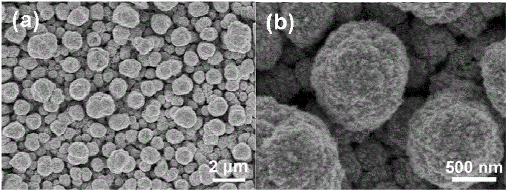
[0037] A gold film is sputtered on the substrate first; wherein, the substrate is a single crystal silicon wafer in a semiconductor, and the thickness of the gold film is 10nm. Then put the graphite as the anode and the substrate covered with the gold film as the cathode in the gold electrolyte, at 30μA / cm 2 Electrodeposition under direct current for 20h; Among them, the gold electrolyte is a mixture of 0.2g / L chloroauric acid solution and 50g / L polyvinylpyrrolidone solution, which is similar to figure 1 The shown array of gold micro-nanostructures. Afterwards, the gold micro-nanostructure array was washed once with deionized water.

Embodiment 2

[0039] The concrete steps of preparation are:

[0040] A gold film is sputtered on the substrate first; wherein, the substrate is a single crystal silicon wafer in a semiconductor, and the thickness of the gold film is 20nm. Then put the graphite as the anode and the substrate covered with the gold film as the cathode in the gold electrolyte, at 130μA / cm 2 Electrodeposition under direct current for 17h; Among them, the gold electrolyte is a mixture of 1.2g / L chloroauric acid solution and 38g / L polyvinylpyrrolidone solution, which is similar to figure 1 The shown array of gold micro-nanostructures. Afterwards, the gold micro-nanostructure array was washed twice with deionized water.

Embodiment 3

[0042] The concrete steps of preparation are:

[0043] A gold film is sputtered on the substrate first; wherein, the substrate is a single crystal silicon wafer in a semiconductor, and the thickness of the gold film is 30nm. Then put the graphite as the anode and the substrate covered with the gold film as the cathode in the gold electrolyte, at 250μA / cm 2 Electrodeposition under the DC current of 14h; Wherein, gold electrolytic solution is the mixed solution of the chloroauric acid solution of 2.5g / L and the polyvinylpyrrolidone solution of 25g / L, makes such as figure 1 The shown array of gold micro-nanostructures. Afterwards, the gold micro-nanostructure array was washed twice with deionized water.


PUM

PropertyMeasurementUnit
Particle sizeaaaaaaaaaa
Thicknessaaaaaaaaaa
Wavelengthaaaaaaaaaa

Abstract

The invention discloses a gold micro-nano structure array and preparation method as well as application thereof. The array comprises a substrate coated with a gold film, a gold microprism array is arranged on the gold film, tops of gold microprisms forming the gold microprism array are hemispheric; each gold microprism with the hemispheric top has the prismdiameter of 200nm-3[mu]m and the prism height of 300nm-6[mu]m, and is composed of gold nano particles; and the particle size of the gold nano particles is 3-30nm. The method comprises the following steps of: firstly, forming the gold film on the substrate through sputtering, then, adding the substrate coated with the gold film into a gold electrolyte as a cathode, performing electrodeposition for 8-20 hours with 30-500[mu]A/cm<2> direct current, wherein, the gold electrolyte is a mixed solution of 0.2-5g/L chloroauric acid solution and 2-50g/L polyvinyl pyrrolidone solution, thereby obtaining the target product. The gold micro-nano structure array can be used as an SERS (Surface Enhanced Raman Scattering) active substrate, and the content of rhodamine or methyl parathion attached on the gold micro-nano structure array is measured through a laser Raman spectrometer.

Description

technical field [0001] The present invention relates to a micro-nano structure array and its preparation method and use, in particular to a gold micro-nano structure array and its preparation method and use. Background technique [0002] Surface-enhanced Raman scattering (SERS) spectroscopy has the advantages of identifying molecular fingerprints, high sensitivity, and fast response, and has a wide range of applications in chemical analysis, biomedicine, and environmental monitoring. For this reason, people have prepared a large amount of precious metal nanostructure SERS substrates, as applicant's entitled "Agnanosheet-assembledmicro-hemispheresaseffectiveSERSsubstrates", ChemicalCommunications, 2011, 47, 2709-2711 ("The micron hemisphere assembled by silver nanosheet serves as effective SERS substrate ", "Chemical Communications", 2011, No. 47, pp. 2709-2711). The product mentioned in this article is assembled into a hemisphere from silver nanosheets with a thickness of 1...

Claims


Application Information

Patent Timeline
IPC IPC(8): B81B1/00B81C1/00B82Y40/00B82Y30/00G01N21/65
Inventor 朱储红孟国文王秀娟
Owner HEFEI INSTITUTES OF PHYSICAL SCIENCE - CHINESE ACAD OF SCI
Why Eureka
Try Eureka