Supercharge Your Innovation With Domain-Expert AI Agents!

A method of forming a germanium channel layer of an nmos transistor device, an nmos transistor device, and a cmos device

A channel layer, transistor technology, applied in transistors, semiconductor devices, electric solid state devices, etc., can solve problems such as poor mobility of standard gate stacks, and achieve the effect of increasing device properties

Active Publication Date: 2019-06-28
INTERUNIVERSITAIR MICRO ELECTRONICS CENT (IMEC VZW)
View PDF8 Cites 0 Cited by
  • Summary
  • Abstract
  • Description
  • Claims
  • Application Information

AI Technical Summary

Problems solved by technology

Poor mobility using standard gate stacks has been widely reported in conventional planar Ge nFETs (e.g. with (100)-Ge as the main carrier transport plane)

Method used


Image

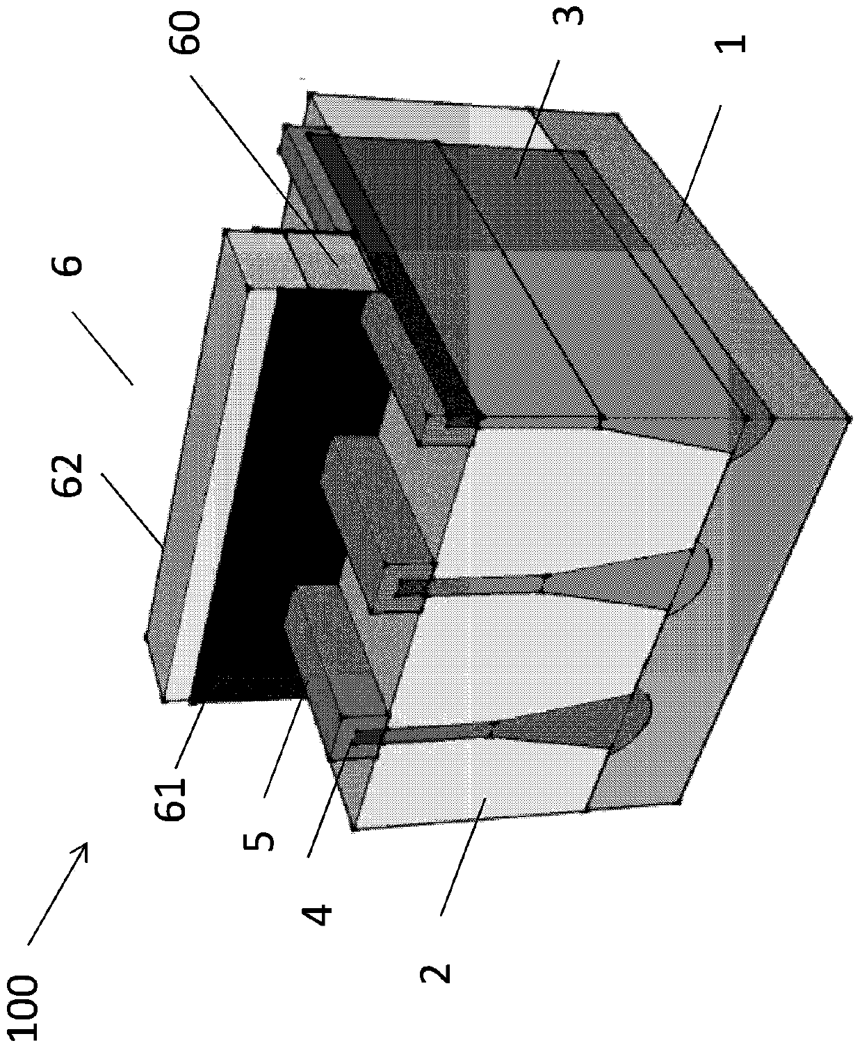
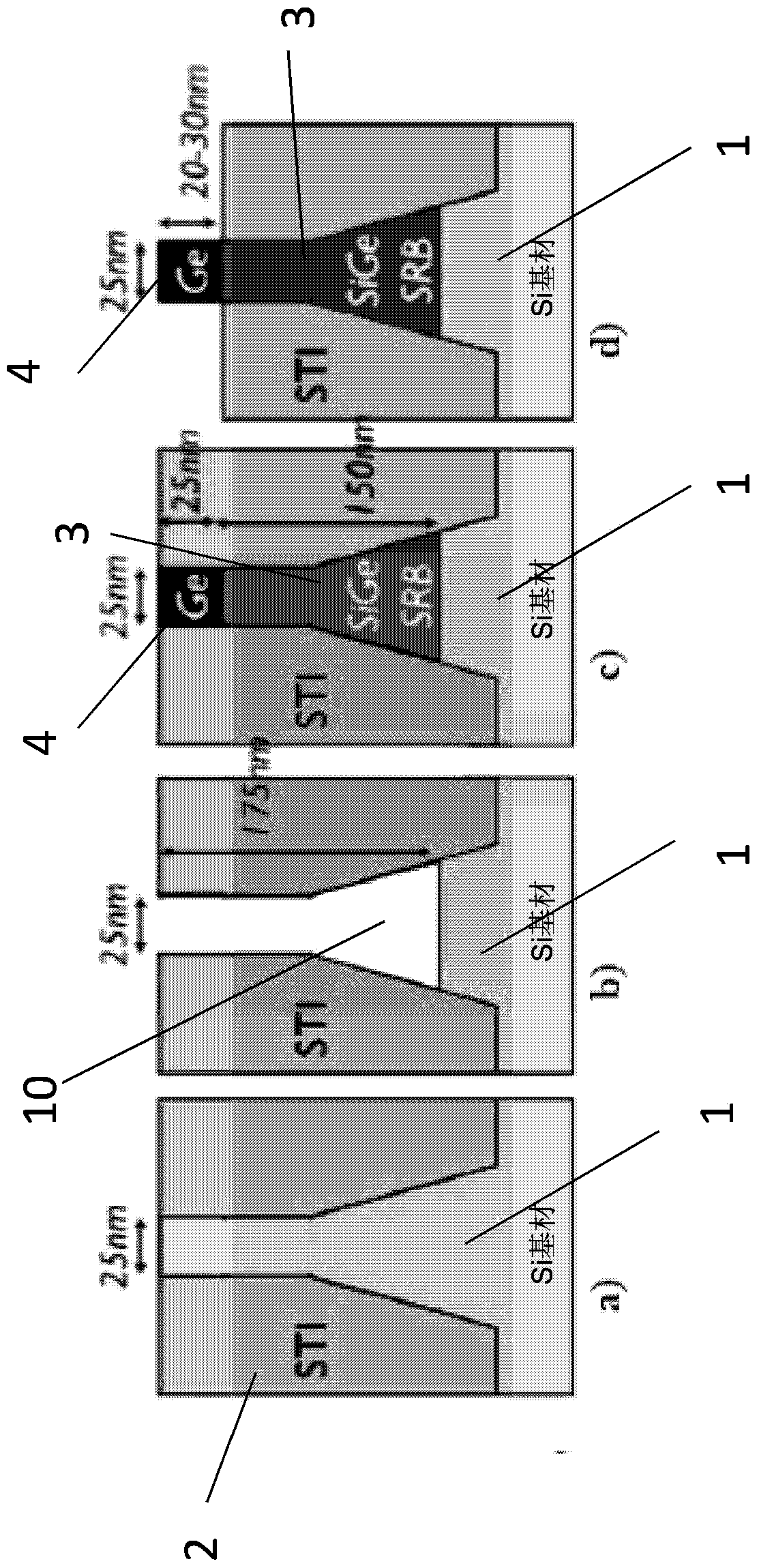
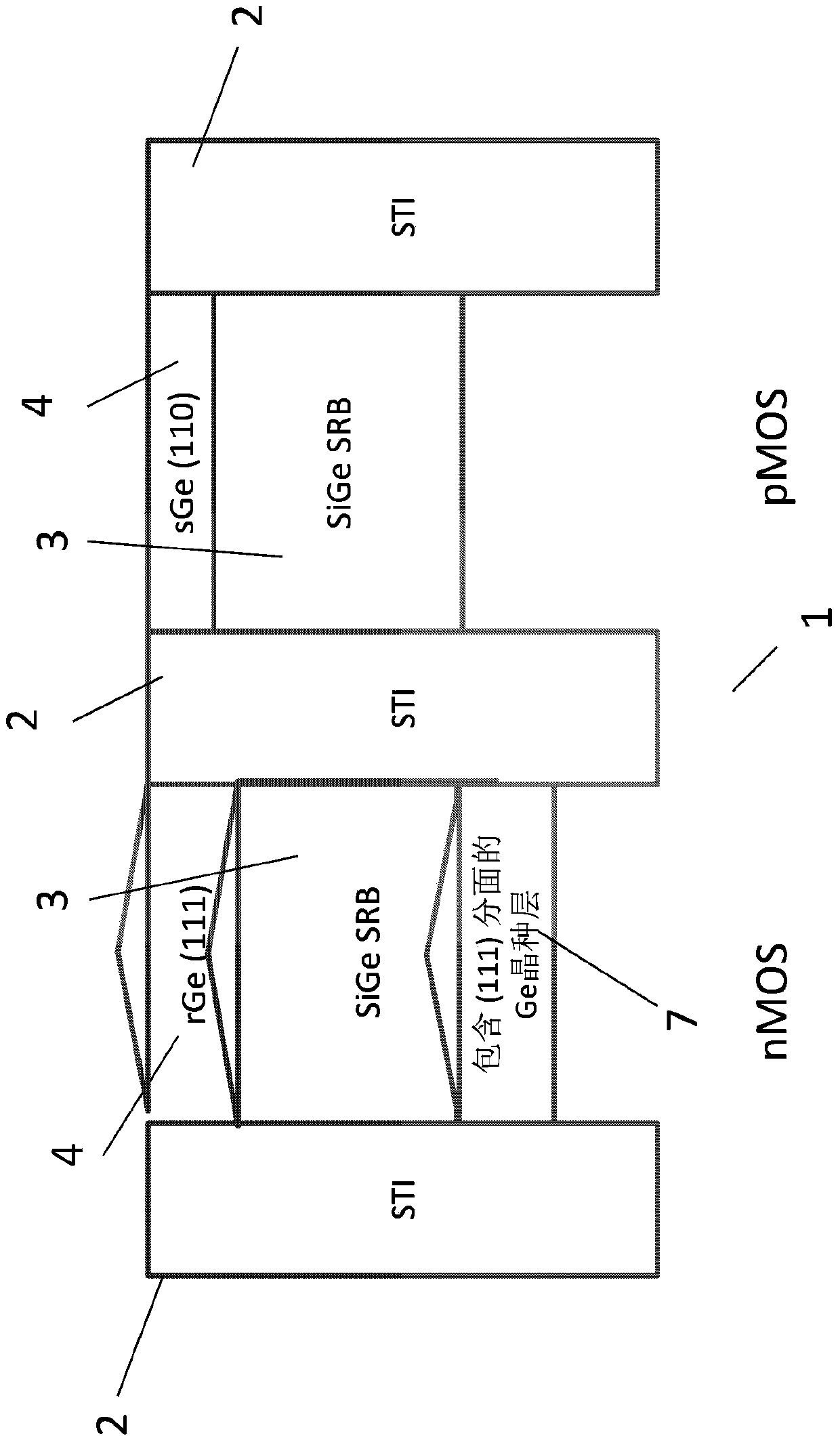
  • A method of forming a germanium channel layer of an nmos transistor device, an nmos transistor device, and a cmos device
  • A method of forming a germanium channel layer of an nmos transistor device, an nmos transistor device, and a cmos device
  • A method of forming a germanium channel layer of an nmos transistor device, an nmos transistor device, and a cmos device

Examples


Embodiment Construction

[0050] DETAILED DESCRIPTION OF THE PREFERRED EMBODIMENTS

[0051] The present invention will be described with respect to specific embodiments and with reference to certain drawings but the invention is not limited thereto but only by the claims. The drawings described are illustrative only and non-limiting. In the drawings, the size of some of the elements may be exaggerated and not drawn to scale for illustrative purposes. The dimensions and relative dimensions do not necessarily correspond to practical simplifications for practicing the invention.

[0052] In addition, in the specification and claims, the terms "first", "second" and "third" are only used to distinguish similar elements, rather than to describe sequence or time sequence. The terms are interchangeable under appropriate circumstances and the embodiments of the invention can operate in other sequences than described and illustrated herein.

[0053] Furthermore, in the description and claims, the terms top,...


PUM


Abstract

A method of forming a germanium channel layer for an NMOS transistor device, the method comprising: a. providing a trench having sidewalls defined by a dielectric material structure and adjoining a surface of a silicon substrate; b. a seed layer is grown in said trench on said surface, said seed layer has a front surface comprising facets with a (111) orientation; c. said crystal in said trench planting a strain relaxation buffer layer on the seed layer, the strain relaxation buffer layer comprising silicon germanium; d. planting a channel layer comprising germanium (Ge) on the strain relaxation buffer layer; and related NMOS transistor devices and CMOS devices .

Description

technical field [0001] The present invention relates to methods of fabricating germanium channel layers of transistor devices, preferably NMOS transistor devices, and related devices. Background technique [0002] In CMOS production, it is often desirable to have a combination of tensile strained / unstrained and compressively strained channel structures for each NOMS and PMOS transistor device on a single substrate. [0003] Prior art solutions are to provide different channel materials for the channel structure (channel layer) for tensile and compressive strain. [0004] The use of channel materials such as Ge-based or III-V-based poses particular problems. At advanced technology nodes, there is an urgent need for channel materials with higher mobility compared to conventional strained and unstrained Si channel reference devices, aiming to further enhance device performance. [0005] Therefore, commercial use of germanium-based channel materials is considered to be state o...

Claims


Application Information

Patent Timeline
Patent Type & Authority Patents(China)
IPC IPC(8): H01L21/336H01L29/78H01L29/10H01L27/092
CPCH01L27/092H01L29/1054H01L29/66522H01L29/7849H01L21/0245H01L21/02516H01L29/66795H01L21/02645H01L21/02532H01L21/02381H01L21/02609H01L29/165H01L21/823814H01L29/045H01L27/0924H01L21/823821H01L21/823807H01L29/7853H01L27/0922H01L29/7848
Inventor J·米塔德R·鲁L·维特斯
Owner INTERUNIVERSITAIR MICRO ELECTRONICS CENT (IMEC VZW)
Features
  • R&D
  • Intellectual Property
  • Life Sciences
  • Materials
  • Tech Scout
  • Unparalleled Data Quality
  • Higher Quality Content
  • 60% Fewer Hallucinations
Learn More