Fingerprint Sensing Device And Fingerprint Sensing Method Thereof

A sensing device and sensing method technology, applied in the direction of acquiring/arranging fingerprints/palmprints, instruments, characters, and pattern recognition, etc., can solve problems such as difficult to correctly identify lines, affect electrode plate sensing, etc., and achieve large signal Dynamic range, prevention of operation noise interference, effects of eliminating parasitic capacitance effects

Inactive Publication Date: 2016-07-06
ELAN MICROELECTRONICS CORPORATION
View PDF3 Cites 21 Cited by
  • Summary
  • Abstract
  • Description
  • Claims
  • Application Information

AI Technical Summary

Problems solved by technology

The parasitic capacitances Cpla, Cp1b, and Cp1c will affect the sensing of the electrode plates 16a, 16b, and 16c. The higher the parasitic capacitances Cpla, Cp1b, and Cp1c, the smaller the dynamic range of the sensing voltage obtained by measuring the electrode plates 16a, 16b, and 16c. , the more difficult it is to correctly identify whether the detected lines are peaks or valleys
In addition, the operation noise of the detection circuits 18a, 18b, 18c will also interfere with the electrode plates 16a, 16b, 16c via the parasitic capacitances Cpla, Cp1b, Cp1c

Method used


Image

  • Fingerprint Sensing Device And Fingerprint Sensing Method Thereof
  • Fingerprint Sensing Device And Fingerprint Sensing Method Thereof
  • Fingerprint Sensing Device And Fingerprint Sensing Method Thereof

Examples


Embodiment Construction

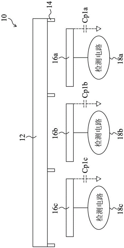
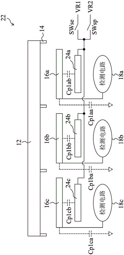
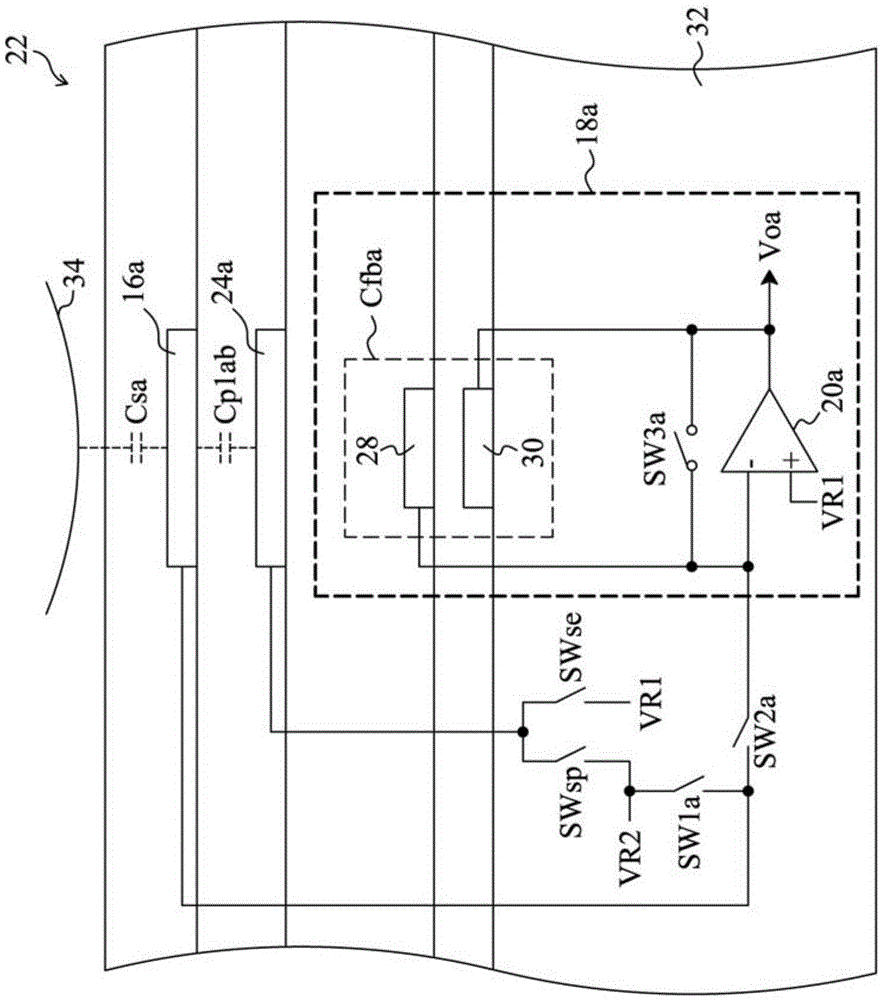
[0043] figure 2 is an embodiment of the fingerprint sensing device 22 of the present invention, which is compatible with figure 1 The fingerprint sensing device 10 also includes a protective layer 12, an electrostatic discharge layer 14, electrode plates 16a, 16b, 16c and detection circuits 18a, 18b, 18c. In addition, the fingerprint sensing device 22 also includes barrier plates 24a, 24b, 24c and switches SWse, SWsp, wherein the barrier plate 24a is between the electrode plate 16a and the detection circuit 18a, and the barrier plate 24b is between the electrode plate 16b and the detection circuit 18b , the barrier plate 24c is between the electrode plate 16c and the detection circuit 18c, one end of the switch SWse is connected to the barrier plates 24a, 24b, 24c, the other end of the switch SWse receives the voltage VR1, and one end of the switch SWsp is connected to the barrier plates 24a, 24b, 24c, The other end of the switch SWsp receives the voltage VR2. In the finger...


PUM


Abstract

A fingerprint sensing device comprises a shielding plate configured between an electrode plate and a detection circuit for reducing a parasitic capacitor between the electrode plate and a conductor thereunder. Consequently, a larger signal dynamic range can be achieved and the electrode plate can be prevented from operation noise interference of the detection circuit. The shielding plate and the electrode plate have the same potential. Accordingly, a parasitic capacitor effect between the shielding plate and the electrode plate can be eliminated. Thus, the fingerprint sensing device of the present invention has a better noise resistibility.

Description

technical field [0001] The invention relates to a fingerprint sensing device and method, in particular to a fingerprint sensing device with low parasitic capacitance and a fingerprint sensing method thereof. Background technique [0002] figure 1 It is a known fingerprint sensing device 10, wherein the protective layer 12 is used for fingers to touch and protect the plurality of electrode plates 16a, 16b, 16c below it, and the electrostatic discharge (Electro-Static Discharge; ESD) layer 14 is used to provide electrostatic discharge protection. A plurality of detection circuits 18a, 18b, 18c are respectively connected to the corresponding electrode plates 16a, 16b, 16c to detect the capacitance between the electrode plates 16a, 16b, 16c and the finger (not shown) to obtain a sensing voltage. Since the fingerprint of a finger is composed of uneven lines, there are peaks and valleys in the fingerprint. In addition, the distances between the crests and troughs of the fingerpr...

Claims


Application Information

Patent Timeline
Patent Type & Authority Applications(China)
IPC IPC(8): G06K9/00
CPCG06V40/1306
Inventor 杨昭锜
Owner ELAN MICROELECTRONICS CORPORATION
Why Eureka
Try Eureka