

pin photodiode, x-ray detection pixel, device and detection method thereof
A photodiode and X-ray technology, applied in measuring devices, X/γ/cosmic radiation measurement, photovoltaic power generation, etc., can solve problems such as dark current of PIN photodiode defects
- Summary
- Abstract
- Description
- Claims
- Application Information
AI Technical Summary
Problems solved by technology
Method used
Image

Examples
Embodiment Construction
[0034] The specific implementations of the PIN photodiode, X-ray detection pixel, device and detection method provided by the embodiments of the present invention will be described in detail below in conjunction with the accompanying drawings.
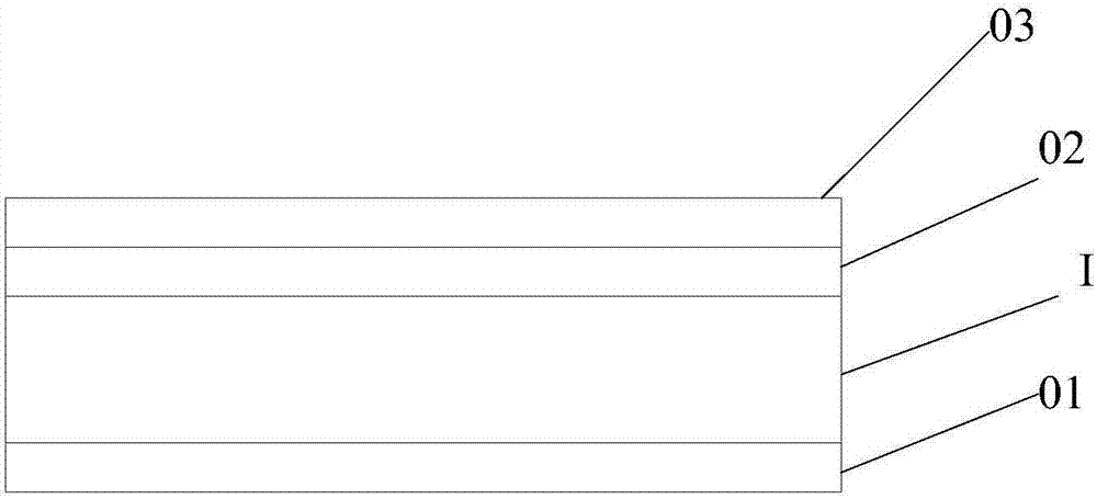
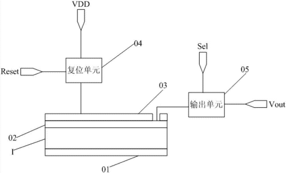
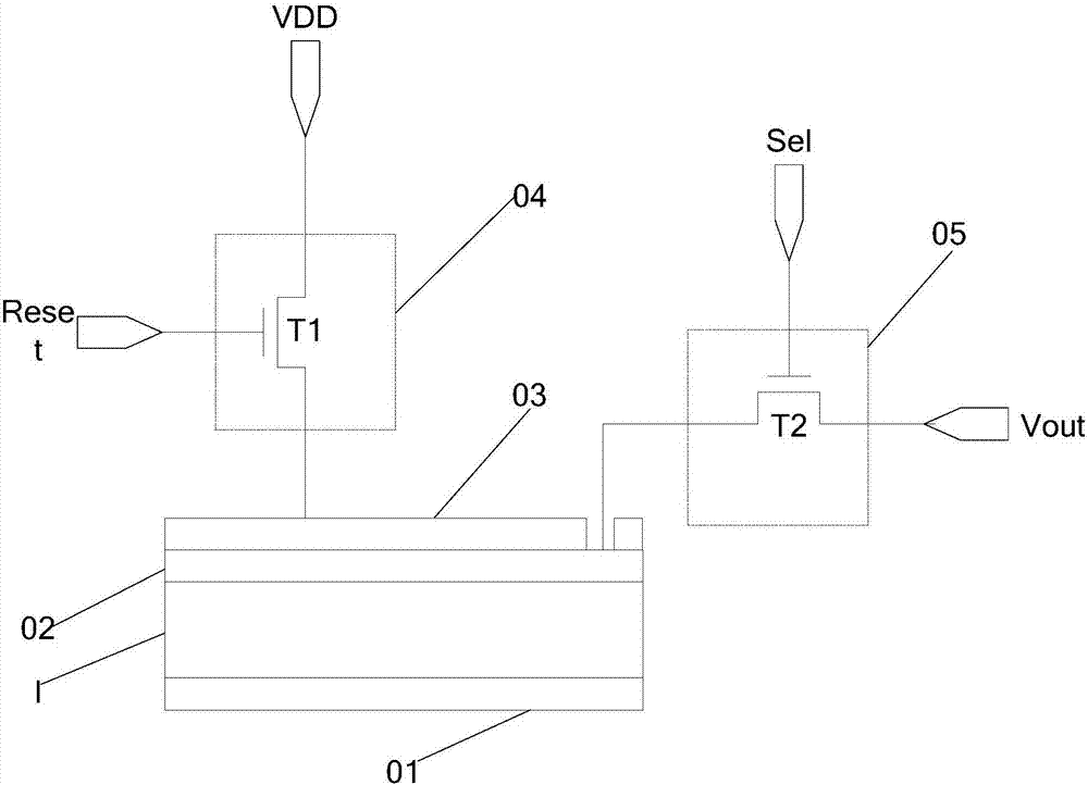
[0035] An embodiment of the present invention provides a PIN photodiode, such as figure 1 As shown, it may include: intrinsic layer I, first doped layer 01 and second doped layer 02; also includes: third doped layer 03; intrinsic layer I is located in first doped layer 01 and second doped layer Between the impurity layers 02 , the third doped layer 03 is located on the second doped layer 02 .
[0036] The above-mentioned PIN photodiode provided by the embodiment of the present invention can prevent the second doped layer from being periodically damaged by covering the second doped layer with a third doped layer, thereby preventing the surface of the second doped layer from The occurrence of defects can improve the defect dark current ...
PUM
 Abstract
Description
Claims
Application Information